P8503BMG
N-Channel Logic Level Enhancement Mode MOSFET
PRODUCT SUMMARY
V(BR)DSS
RDS(ON)
30V 85mΩ @VGS = 10V
ID 2.4A
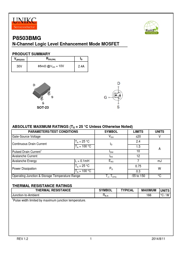
SOT-23
ABSOLUTE MAXIMUM RATINGS (TA = 25 °C Unless Otherwise Noted)
PARAMETERS/TEST CONDITIONS
SYMBOL
LIMITS
Gate-Source Voltage
VGS ±20
Continuous Drain Current Pulsed Drain Current1
TA = 25 °C TA = 100 °C
ID IDM
2.4 1.5 10
Avalanche Current
IAS 12
Avalanche Energy
L = 0.1m H
Power Dissipation
TA = 25 °C TA = 100 °C
0.75 0.3
Operating Junction & Storage Temperature Range
TJ, TSTG
-55 to 150
UNITS V
A m J W °C
THERMAL RESISTANCE RATINGS
THERMAL RESISTANCE Junction-to-Ambient 1Pulse width limited by maximum junction temperature.
SYMBOL Rq JA
TYPICAL
MAXIMUM UNITS 166 °C / W
REV 1.2
1 2014/8/11
N-Channel Logic Level Enhancement Mode MOSFET
ELECTRICAL CHARACTERISTICS (TJ = 25 °C, Unless Otherwise...