UNIVERSAL MICROELECTRONICS AD14CD300
Active Delay Lines
| Part No. | AD14CD300 |
|---|---|
| Datasheet | AD14CD300 Download |
| Manufacturer |  UNIVERSAL MICROELECTRONICS |
| Description | Active Delay Lines |
| Buy | Stock & Price |
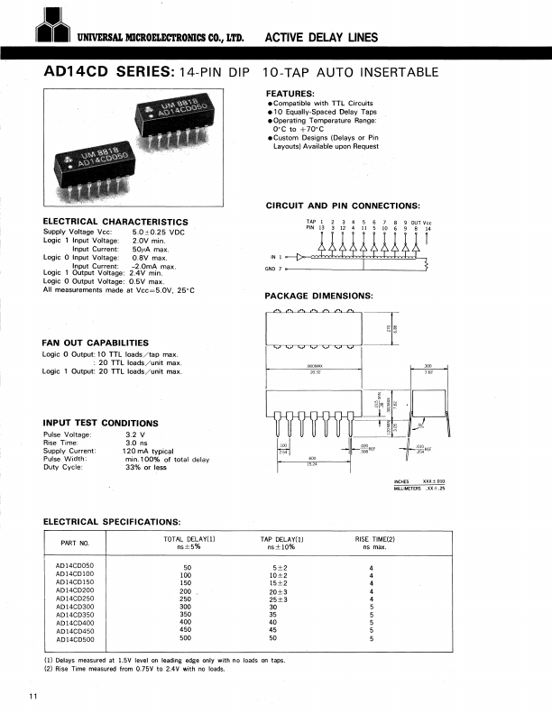
FEATURES
:●Compatible with TTL Circuits e 10 Equally-Spaced Delay Taps
●Operating Temperature Range: o●c to +1o●c eCustom Designs (Delays or Pin Layouts) Available upon Request
ELECTRICAL CHARACTERISTICS
Supply Voltage Vee: 5.0±0.25 VDC Logic 1 Input Voltage: 2.0V min. Input Current: 50µA max. Logic 0 Input Voltage: O.BV max. Input Current: -2.0mA max. Logic 1 Output Voltage: 2.4V min. Logic 0 Output Voltage: 0.5V max. All measurements made at Vcc=5.0V, 25°C FAN OUT CAPABILITIES Logic 0 Output: 10 TTL loads/tap max. : 20 TTL loads/unit max. Logic 1 Output: 20 TTL loads/unit max. CIRCUIT AND PIN CONNECTIONS: TAP I 2 3 4 5 6 7 8 9 OUT Vee PIN 13 3 12 4 11 5 10 6 9 8 14 ":: ~HH!HH~ PACKAGE DIMENSIONS: I~~~~:::[] I~I ~ INPUT TEST CONDITIONS Pulse Voltage: 3.2 v Rise Time: 3.0 ns Supply Current: Pulse Width". 120 mA typical min. 100% of total delay Duty Cycle: 33% or less -H-::●EF .600 i-------,1=5.2"""4- - - - - t -~;;~; ,) _...rso 1~~1£●EF. INCHES XXX±.010 MILLIMETERS●XX ± .25