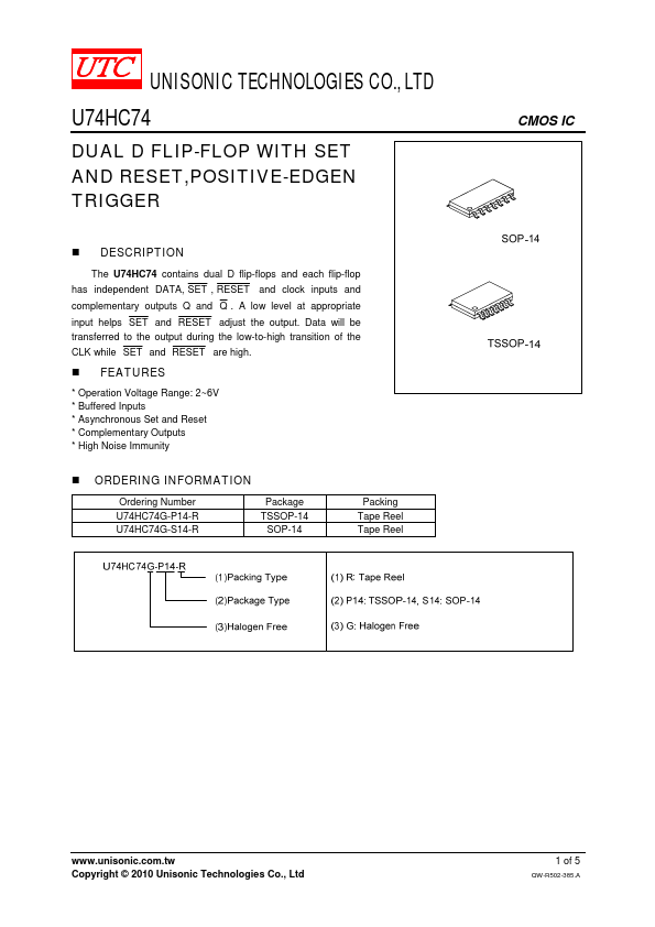
DESCRIPTION
A low level at appropriate input helps SET and RESET adjust the output. Data will be transferred to the output during the low-to-high transition of the CLK while SET and RESET are high. FEATURES
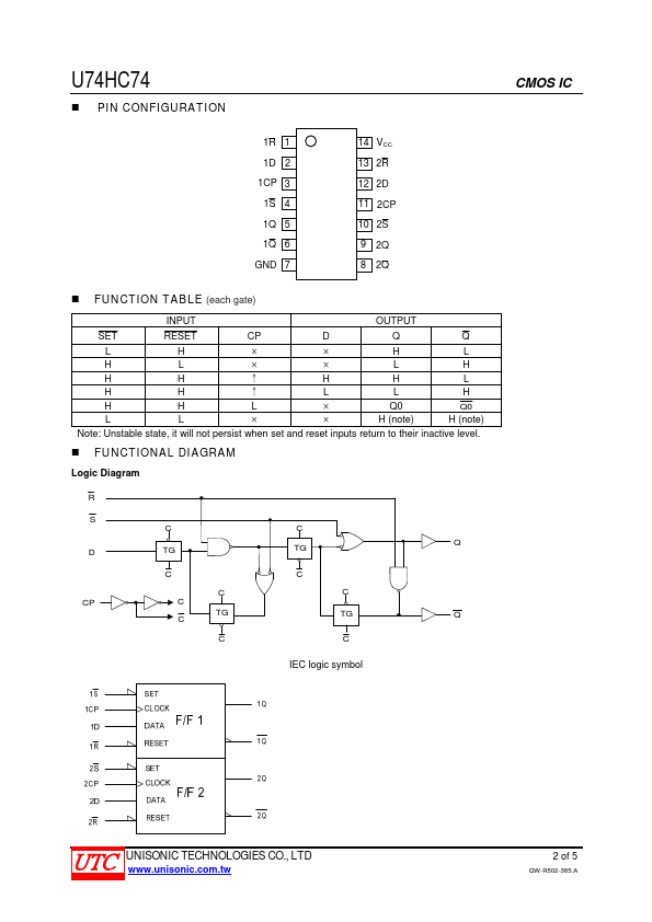
* Operation Voltage Range: 2~6V * Buffered Inputs * Asynchronous Set and Reset * Complementary Outputs * High Noise Immunity ORDERING INFORMATION Ordering Number U74HC74G-P14-R U74HC74G-S14-R Package TSSOP-14 SOP-14 Packing Tape Reel Tape Reel CMOS IC Copyright © 2010 Unisonic Technologies Co., Ltd 1 of 5 QW-R502-385.A U74HC74 PIN CONFIGURATION 1R 1 1D 2 1CP 3 1S 4 1Q 5 1Q 6 GND 7 14 VCC 13 2R 12 2D 11 2CP 10 2S 9 2Q 8 2Q FUNCTION TABLE (each gate) INPUT OUTPUT SET RESET CP D Q Q L H × ×HL H L × × LH H H ↑HHL H H↑LLH H H L × Q0 Q0 L L × × H (note) H (note) Note: Unstable state, it will not persist when set and reset inputs return to their inactive level. FUNCTIONAL DIAGRAM Logic Diagram R S C D TG C TG CC C CP C C TG C TG CC Q Q IEC logic symbol CMOS IC UNISONIC TECHNOLOGI... Unisonic Technologies