Unisonic Technologies U74HCT367
The U74HCT367 is a hex buffer with 3-state outputs. The device is configured into two banks, one with four drivers and one with two drivers, each controlled by its own output enable pin.| Part No. | U74HCT367 |
|---|---|
| Datasheet | U74HCT367 Download |
| Manufacturer |  Unisonic Technologies |
| Description | HEX BUFFERS AND LINE DRIVERS |
| Buy | Stock & Price |
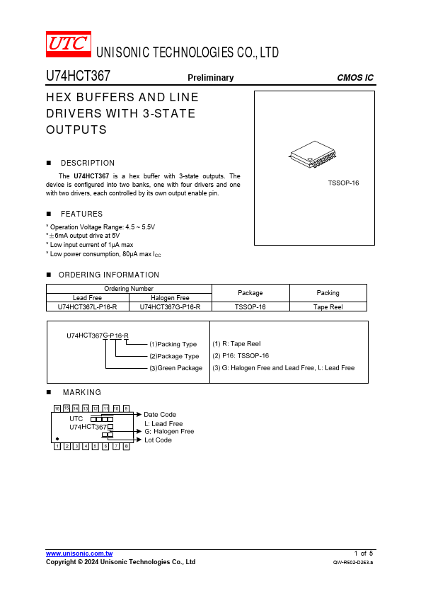
DESCRIPTION
●FEATURES
* Operation Voltage Range: 4.5 ~ 5.5V *±6mA output drive at 5V * Low input current of 1µA max * Low power consumption, 80µA max ICC● ORDERING INFORMATION Ordering Number Lead Free Halogen Free U74HCT367L-P16-R U74HCT367G-P16-R Package TSSOP-16 CMOS IC Packing Tape Reel
● MARKING Copyright © 2024 Unisonic Technologies Co., Ltd 1 of 5 QW-R502-D263.a U74HCT367
● PIN CONFIGURATION Preliminary CMOS IC
● FUNCTION TABLE INPUT( ΟΕ ) INPUT(A) OUTPUT(Y) L L L L H H H X Z Note: H: HIGH voltage level; L: LOW voltage level; X=don’t care; Z=high-impedance OFF-state.
● LOGIC DIAGRAM (Positive Logic) UNISONIC TECHNOLOGIES CO., LTD 2 of 5 QW-R502-D263.a U74HCT367 Preliminary CMOS IC
●
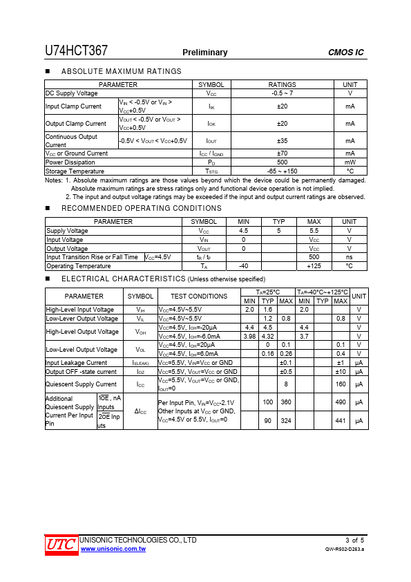
ABSOLUTE MAXIMUM RATINGS
PARAMETER SYMBOL RATINGS UNIT DC Supply Voltage VCC -0.5 ~ 7 V Input Clamp Current VIN < -0.5V or VIN > VCC+0.5V IIK ±20 mA Output Clamp Current VOUT < -0.5V or VOUT > VCC+0.5V IOK ±20 mA Continuous Output Current -0.5V < VOUT < VCC+0.5V IOUT ±35 mA VCC or Ground Current ICC / IGND ±70 mA Power Dissipation PD 500 mW Storage Temperature TSTG -65 ~ +150 °C Notes: 1.