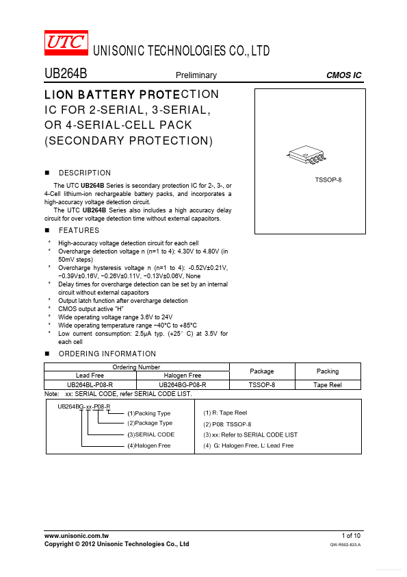
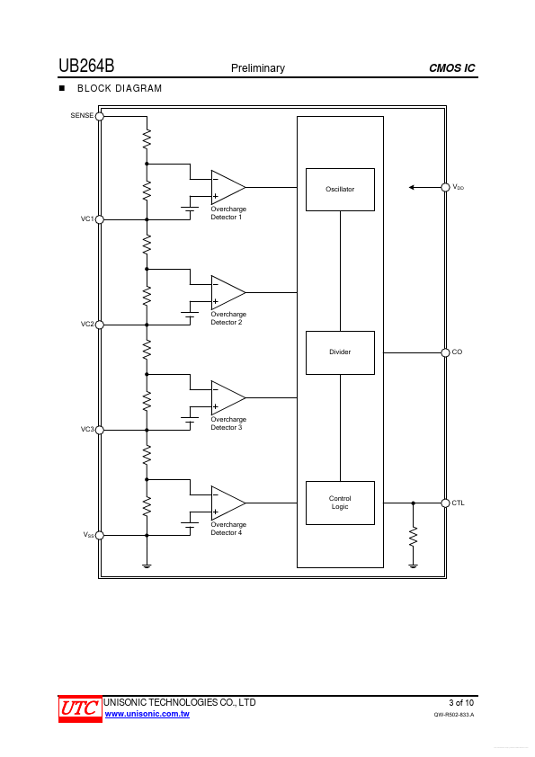
DESCRIPTION
* * * * * * * * * FEATURES
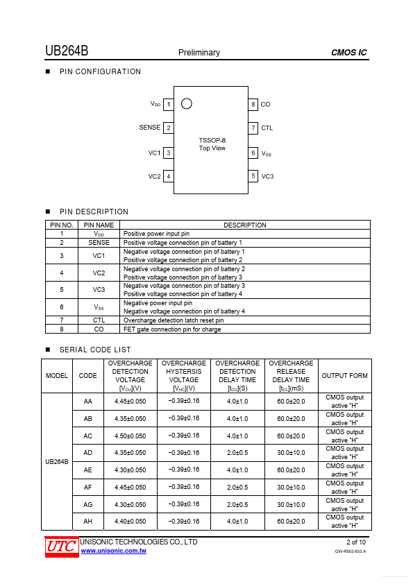
High-accuracy voltage detection circuit for each cell Overcharge detection voltage n (n=1 to 4): 4.30V to 4.80V (in 50mV steps) Overcharge hysteresis voltage n (n=1 to 4): -0.52V±0.21V, −0.39V±0.16V, −0.26V±0.11V, −0.13V±0.06V, None Delay times for overcharge detection can be set by an internal circuit without external capacitors Output latch function after overcharge detection CMOS output active “H” Wide operating voltage range 3.6V to 24V Wide operating temperature range −40°C to +85°C Low current consumption: 2.5μA typ. (+25°C) at 3.5V for each cell ORDERING INFORMATION Ordering Number Lead Free Halogen Free UB264BL-P08-R UB264BG-P08-R xx: SERIAL CODE, refer SERIAL CODE LIST. Package TSSOP-8 Packing Tape Reel Note: Copyright © 2012 Unisonic Technologies Co., Ltd 1 of 10 QW-R502-833.A Free Datasheet UB264B PIN CONFIGURATION Preliminary CMOS IC PIN DESCRIPTION
PIN NAME VDD SENSE VC1 VC2 VC3 VSS CTL CO DESCRIPTION
Positive power input pin... Unisonic Technologies