CHA2190-99F
Overview
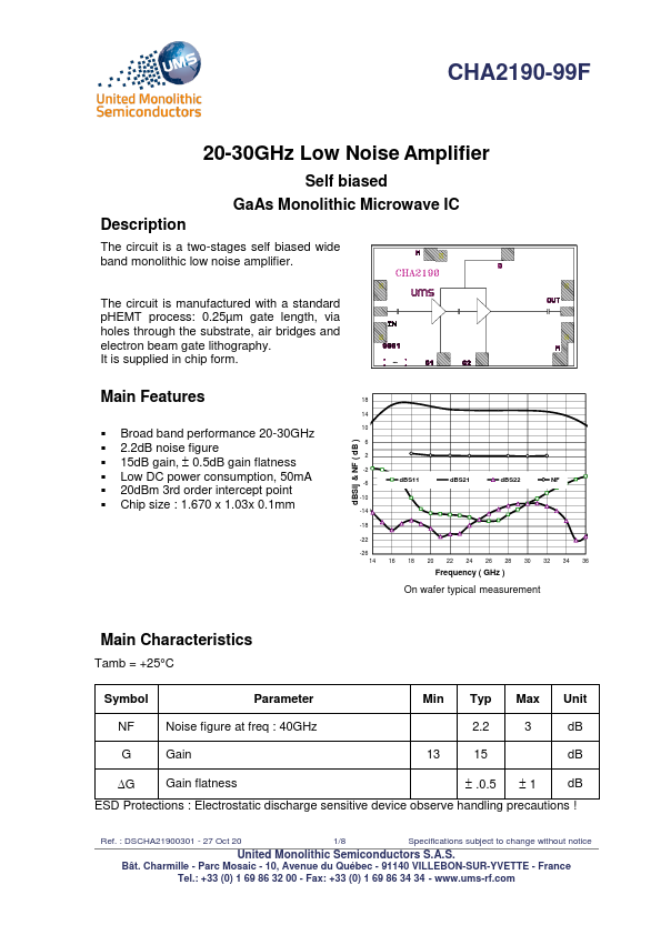
GaAs Monolithic Microwave IC The circuit is a two-stages self biased wide band monolithic low noise amplifier. The circuit is manufactured with a standard pHEMT process: 0.25µm gate length, via holes through the substrate, air bridges and electron beam gate lithography.
- Broad band performance 20-30GHz
- 2.2dB noise figure
- 15dB gain, 0.5dB gain flatness
- Low DC power consumption, 50mA
- 20dBm 3rd order intercept point
- Chip size : 1.670 x 1.03x 0.1mm dBSij & NF ( dB ) 18 14 10 6 2 -2 -6 dBS11 dBS21 dBS22 NF -10 -14 -18 -22 -26 14 16 18 20 22 24 26 28 30 32 34 36 Frequency ( GHz ) On wafer typical measurement Main Characteristics Tamb = +25°C Symbol Parameter Min Typ Max Unit NF Noise figure at freq : 40GHz
- 2 3 dB G Gain 13 15 dB G Gain flatness .0.5 1 dB ESD Protections : Electrostatic discharge sensitive device observe handling precautions ! Ref. : DSCHA21900301 - 27 Oct 20 1/8