CHA2193-99F
Overview
The CHA2193-99F is a three stages low noise amplifier. It is designed for a wide range of applications, from military to commercial communication systems.
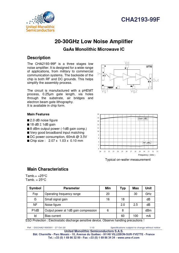
- 2.0 dB noise figure
- 18 dB 1dB gain
- 8 dBm output power (-1dB gain comp.)
- Very good broadband input matching
- DC power consumption, 60mA @ 3.5V
- Chip size : 2.07 x 1.03 x 0.10 mm 20 18 Gain (dB) 16 14 12 10 8 6 4 NF (dB) 2