Datasheet4U Logo Datasheet4U.com

CHA3666-99F - Low Noise Amplifier

Datasheet Summary

Description

wide band monolithic low noise amplifier.

The circuit is manufactured with a standard pHEMT process: 0.25µm gate length, via holes through the substrate, air bridges and RFin electron beam gate lithography.

Features

  • Broadband performances: 6-17GHz.
  • 1.8dB noise figure.
  • 26dBm 3rd order intercept point.
  • 17dBm power at 1dB compression.
  • 21dB gain.
  • Low DC power consumption.
  • DC bias: Vd=4.0Volt@Id=80mA.
  • Chip size 1.47x1.47x0.1mm 24,0 22,0 20,0 18,0 Gain 16,0 14,0 12,0 10,0 8,0 6,0 4,0 2,0 NF 0,0 4,00 6,00 8,00 10,00 12,00 14,00 16,00 18,00 Main Electrical Characteristics Tamb. = +25°C, Vd1=Vd2= +4V Pads: P1, N2=GND Symbol Parameter Min Typ Max Unit Fop.

📥 Download Datasheet

Datasheet preview – CHA3666-99F

Datasheet Details

Part number CHA3666-99F
Manufacturer United Monolithic Semiconductors
File Size 489.05 KB
Description Low Noise Amplifier
Datasheet download datasheet CHA3666-99F Datasheet
Additional preview pages of the CHA3666-99F datasheet.
Other Datasheets by United Monolithic Semiconductors

Full PDF Text Transcription

Click to expand full text
CHA3666-99F 6-17GHz Low Noise Amplifier GaAs Monolithic Microwave IC Description 
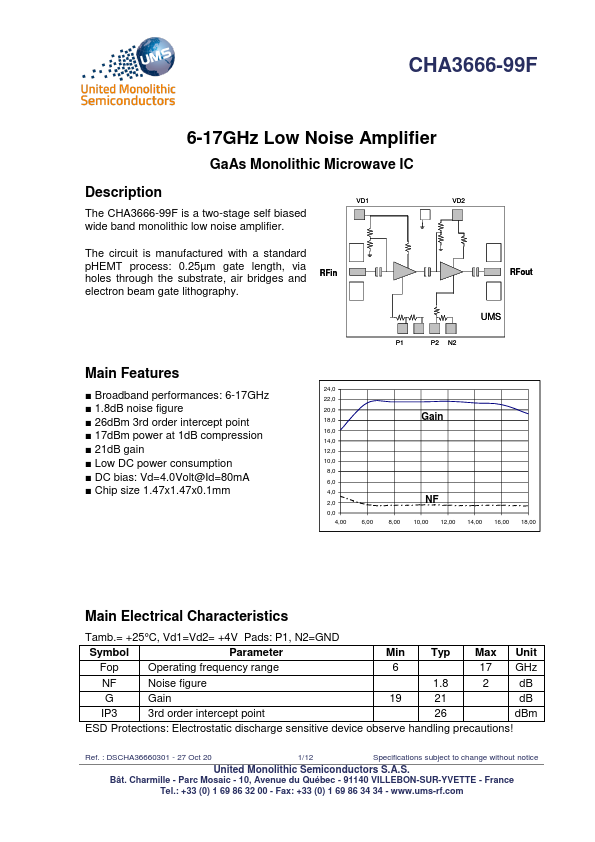
VD1 VD2 The CHA3666-99F is a two-stage self biased wide band monolithic low noise amplifier. The circuit is manufactured with a standard pHEMT process: 0.25µm gate length, via holes through the substrate, air bridges and RFin electron beam gate lithography. RFout UMS P1 P2 N2 Main Features ■ Broadband performances: 6-17GHz ■ 1.8dB noise figure ■ 26dBm 3rd order intercept point ■ 17dBm power at 1dB compression ■ 21dB gain ■ Low DC power consumption ■ DC bias: Vd=4.0Volt@Id=80mA ■ Chip size 1.47x1.47x0.1mm 24,0 22,0 20,0 18,0 Gain 16,0 14,0 12,0 10,0 8,0 6,0 4,0 2,0 NF 0,0 4,00 6,00 8,00 10,00 12,00 14,00 16,00 18,00 Main Electrical Characteristics Tamb.
Published: |