Datasheet4U Logo Datasheet4U.com

CHX1162-QDG - Frequency Multiplier

General Description

The CHX1162-QDG is a packaged monolithic time two multiplier which integrates input and output buffer.

This circuit is a very versatile multiplier for telecommunication and specifically for E-band LO chain.

Moreover it is proposed in standard surface mount package and integrates ESD protection.

Key Features

  • 15 10 Pin= +1dBm 5.
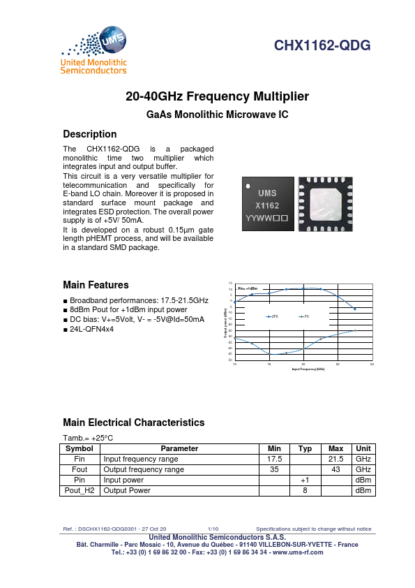
  • Broadband performances: 17.5-21.5GHz 0 Output power (dBm).
  • 8dBm Pout for +1dBm input power -5 -10.
  • DC bias: V+=5Volt, V- = -5V@Id=50mA -15 -20.
  • 24L-QFN4x4 -25 2F0 F0 -30 -35 -40 -45 -50 16 18 20 22 24 Input Frequency (GHz) Main Electrical Characteristics Tamb. = +25°C Symbol Parameter Fin Input frequency range Fout Output frequency range Pin Input power Pout_H2 Output Power Min Typ Max Unit 17.5 21.5 GHz 35 43 GHz +1.

📥 Download Datasheet

Datasheet Details

Part number CHX1162-QDG
Manufacturer United Monolithic Semiconductors
File Size 354.60 KB
Description Frequency Multiplier
Datasheet download datasheet CHX1162-QDG Datasheet

Full PDF Text Transcription (Reference)

The following content is an automatically extracted verbatim text from the original manufacturer datasheet and is provided for reference purposes only.

View original datasheet text
CHX1162-QDG 20-40GHz Frequency Multiplier GaAs Monolithic Microwave IC Description The CHX1162-QDG is a packaged monolithic time two multiplier which integrates input and output buffer. This circuit is a very versatile multiplier for telecommunication and specifically for E-band LO chain. Moreover it is proposed in standard surface mount package and integrates ESD protection. The overall power supply is of +5V/ 50mA. It is developed on a robust 0.15µm gate length pHEMT process, and will be available in a standard SMD package. Main Features 15 10 Pin= +1dBm 5 ■ Broadband performances: 17.5-21.