CHX2089-99F Overview
Description
The CHX2089-99F is a cascadable times 2 frequency multiplier monolithic circuit. It is designed for a wide range of applications, from ISM to commercial communication systems.
Key Features
- Broadband performances: 8-11.5GHz
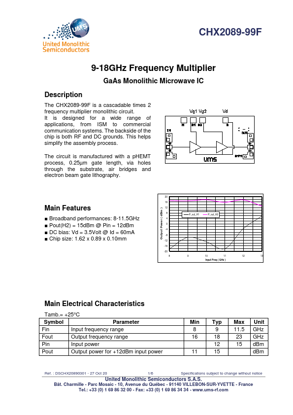
- Pout(H2) = 15dBm @ Pin = 12dBm
- DC bias: Vd = 3.5Volt @ Id = 60mA
- Chip size: 1.62 x 0.89 x 0.10mm Output Power ( dBm ) 20 16 12 8 P_out_H1 P_out_H2 4 0
- 10, Avenue du Québec