CHX2092a99F Overview
Description
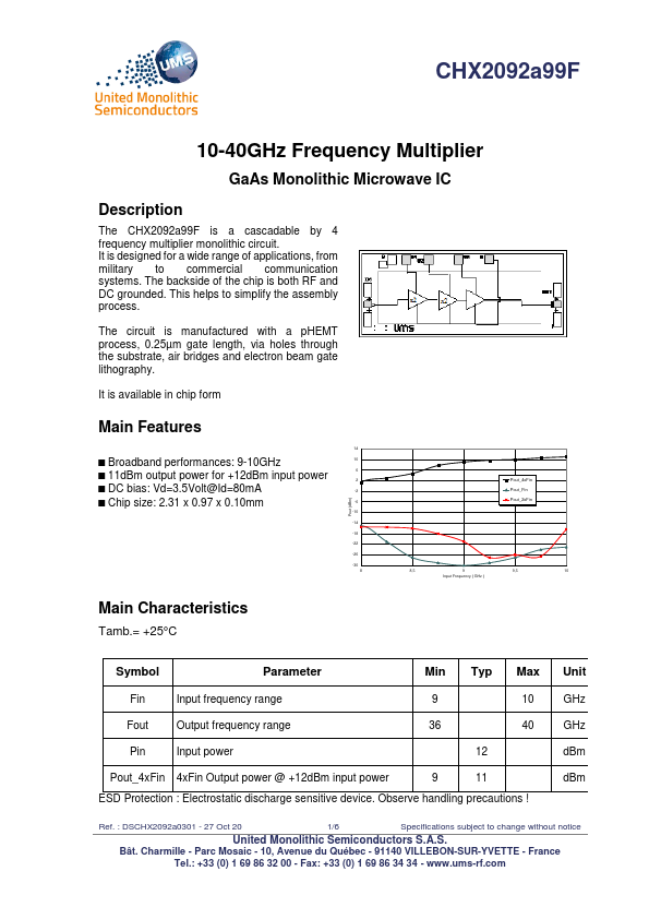
The CHX2092a99F is a cascadable by 4 frequency multiplier monolithic circuit. It is designed for a wide range of applications, from military to commercial communication systems.
Key Features
- Broadband performances: 9-10GHz 10 6
- 11dBm output power for +12dBm input power 2
- DC bias: Vd=3.5Volt@Id=80mA
- Chip size: 2.31 x 0.97 x 0.10mm
- 10 Pout (dBm)
- 10, Avenue du Québec
- 91140 VILLEBON-SUR-YVETTE