Datasheet4U Logo Datasheet4U.com

CHX2193-99F - Frequency Multiplier

General Description

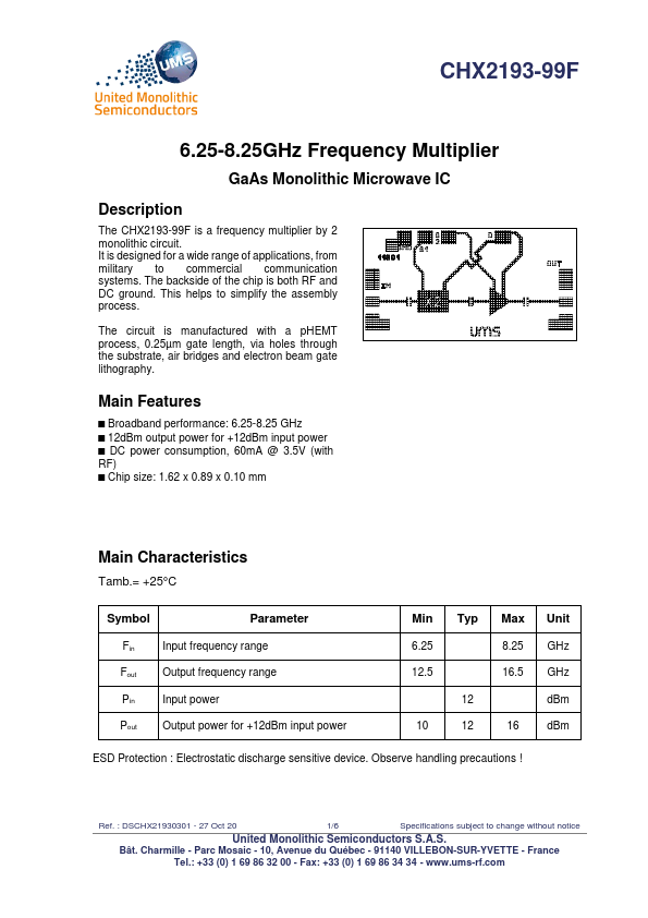
The CHX2193-99F is a frequency multiplier by 2 monolithic circuit.

It is designed for a wide range of applications, from military to commercial communication systems.

The backside of the chip is both RF and DC ground.

Key Features

  • Broadband performance: 6.25-8.25 GHz.
  • 12dBm output power for +12dBm input power.
  • DC power consumption, 60mA @ 3.5V (with RF).
  • Chip size: 1.62 x 0.89 x 0.10 mm Main Characteristics Tamb. = +25°C Symbol Parameter Fin Input frequency range Fout Output frequency range Pin Input power Pout Output power for +12dBm input power Min Typ Max Unit 6.25 8.25 GHz 12.5 16.5 GHz 12 dBm 10 12 16 dBm ESD Protection : Electrostatic discharge sensitive device. Observe handli.

📥 Download Datasheet

Datasheet Details

Part number CHX2193-99F
Manufacturer United Monolithic Semiconductors
File Size 130.51 KB
Description Frequency Multiplier
Datasheet download datasheet CHX2193-99F Datasheet

Full PDF Text Transcription (Reference)

The following content is an automatically extracted verbatim text from the original manufacturer datasheet and is provided for reference purposes only.

View original datasheet text
CHX2193-99F 6.25-8.25GHz Frequency Multiplier GaAs Monolithic Microwave IC Description The CHX2193-99F is a frequency multiplier by 2 monolithic circuit. It is designed for a wide range of applications, from military to commercial communication systems. The backside of the chip is both RF and DC ground. This helps to simplify the assembly process. The circuit is manufactured with a pHEMT process, 0.25µm gate length, via holes through the substrate, air bridges and electron beam gate lithography. Main Features ■ Broadband performance: 6.25-8.25 GHz ■ 12dBm output power for +12dBm input power ■ DC power consumption, 60mA @ 3.5V (with RF) ■ Chip size: 1.62 x 0.89 x 0.10 mm Main Characteristics Tamb.