HM8810A
FEATURES
- Halogen-free Option Available
- Trench FET® Power MOSFETs
- 100 % Rg Tested
- pliant to Ro HS Directive 2002/95/EC
Pb-free Available
Ro HS-
PLIANT
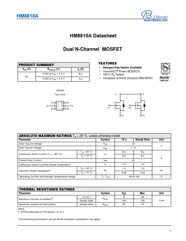
TSOP6 Top View
S1 1 6 D1/D2 2 5
S2 3 4
G1 D1/D2 G2
G1
G2
S1
S2
ABSOLUTE MAXIMUM RATINGS TA = 25 °C, unless otherwise noted
Parameter
Symbol
10 s
Steady State
Unit
Drain-Source Voltage Gate-Source Voltage
± 12
Continuous Drain Current (TJ = 150 °C)a Pulsed Drain Current
TA = 25 °C TA = 70 °C
Continuous Source Current (Diode Conduction)a
Maximum Power Dissipationa
TA = 25 °C TA = 70 °C
Operating Junction and Storage Temperature Range
TJ, Tstg
- 55 to...