VBsemi Electronics N7408
The DFN 3X x 3 is a leadless package. The end of the lead terminal is exposed copper (not plated) as a result of the singulation process in manufacturing.| Part No. | N7408 |
|---|---|
| Datasheet | N7408 Download |
| Manufacturer | VBsemi Electronics |
| Description | N-Channel 30V MOSFET |
| Buy | Stock & Price |
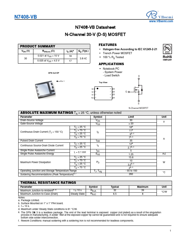
FEATURES
● Halogen-free According to IEC 61249-2-21● Trench Power MOSFET
● 100 % Rg Tested
APPLICATIONS
● Notebook PC - System Power - Load Switch D Top View 1 8 2 7 G 3 6 4 5 S N-Channel MOSFETABSOLUTE MAXIMUM RATINGS
TA = 25 °C, unless otherwise noted Parameter Symbol Limit Unit Drain-Source Voltage Gate-Source Voltage VDS 30 V VGS ± 20 TC = 25 °C 18a Continuous Drain Current (TJ = 150 °C) TC = 70 °C TA = 25 °C ID 11a 9b, c Pulsed Drain Current TA = 70 °C 7b, c A IDM 35 Continuous Source-Drain Diode Current TC = 25 °C TA = 25 °C IS 12a 2.7b, c Single Pulse Avalanche Current L = 0.1 mH IAS 5 Single Pulse Avalanche Energy EAS 1.25 mJ TC = 25 °C 15.6 Maximum Power Dissipation TC = 70 °C TA = 25 °C PD 10 3.2b, c W TA = 70 °C 2b, c Operating Junction and Storage Temperature Range Soldering Recommendations (Peak Temperature)e, f TJ, Tstg - 55 to 150 260 °C THERMAL RESISTANCE RATINGS Parameter Maximum Junction-to-Ambientb, d Maximum Junction-to-Case (Drain) t ≤ 10 s Steady State Symbol RthJA RthJC Typical 32 6.5 Maximum 39 8 Unit °C/W Notes: a.