P4015S
Overview
- Trench Power MOSFET
- Package with Low Thermal Resistance
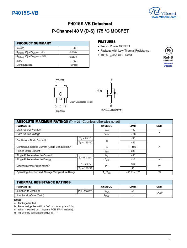
- 100%R g and UIS Tested TO-252 S G GDS Top View Drain Connected to Tab
- P-Channel MOSFET
| Part Number | Manufacturer | Description |
|---|---|---|
| KEH-P4010RB | Pioneer | Multi CD Control High Power Cassette Player |
| P401 | International Rectifier | PASSIVATED ASSEMBLED CIRCUIT ELEMENTS |
| KEH-P4010R | Pioneer | Multi CD Control High Power Cassette Player |
| KEH-P4013R | Pioneer | Multi CD Control High Power Cassette Player |
| KEH-P4013R | Pioneer | Cassette Player with RDS Tuner |