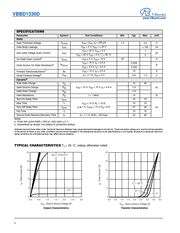
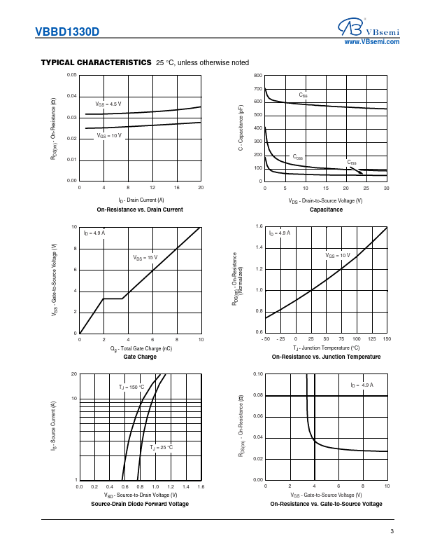
VBsemi Electronics VBBD1330D
The DFN3Xx2 is a leadless package. The end of t he lead terminal is exposed copper (not plated) as a result of the singulation process in manufacturing.| Part No. | VBBD1330D |
|---|---|
| Datasheet | VBBD1330D Download |
| Manufacturer | VBsemi Electronics |
| Description | N-Channel MOSFET |
| Buy | Stock & Price |
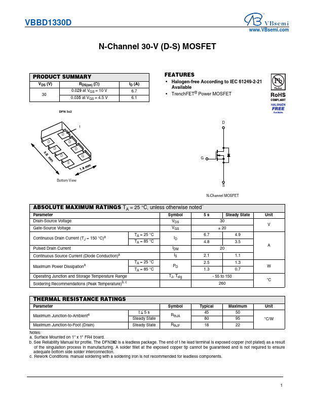
FEATURES
● Halogen-free According to IEC 61249-2-21 Available● TrenchFET® Power MOSFET D G Bottom View S N-Channel MOSFET
ABSOLUTE MAXIMUM RATINGS
TA = 25 °C, unless otherwise noted´ Parameter Symbol 5s Steady State Unit Drain-Source Voltage Gate-Source Voltage VDS 30 V VGS ± 20 Continuous Drain Current (TJ = 150 °C)a Pulsed Drain Current TA = 25 °C TA = 85 °C ID 6.7 4.9 4.8 3.5 A IDM 20 Continuous Source Current (Diode Conduction)a IS 2.1 1.1 Maximum Power Dissipationa TA = 25 °C TA = 85 °C PD 2.5 1.3 1.3 0.7 W Operating Junction and Storage Temperature Range Soldering Recommendations (Peak Temperature)b, c TJ, Tstg - 55 to 150 °C 260 THERMAL RESISTANCE RATINGS Parameter Symbol Typical Maximum Unit Maximum Junction-to-Ambienta Maximum Junction-to-Foot (Drain) t≤5s 45 Steady State RthJA 80 Steady State RthJF 18 50 95 °C/W 22 Notes: a. Surface Mounted on 1" x 1" FR4 board. b. See Reliability Manual for profile. The DFN3Xx2 is a leadless package. A solder fillet at the exposed copper tip cannot be guaranteed and is not required to ensure adequate bottom side solder interconnection. c.