FEATURES
● TrenchFET® power MOSFET APPLICATIONS
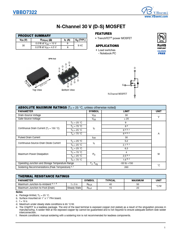
● Load switches - Notebook PC D 1.9 mm 1 3.0 mm Top View 1 4 3 D 2 D D G Bottom View G N-Channel MOSFET S ABSOLUTE MAXIMUM RATINGS
(TA = 25 °C, unless otherwise noted) PARAMETER SYMBOL Drain-Source Voltage Gate-Source Voltage Continuous Drain Current (TJ = 150 °C) Pulsed Drain Current TC = 25 °C TC = 70 °C TA = 25 °C TA = 70 °C Continuous Source-Drain Diode Current TC = 25 °C TA = 25 °C TC = 25 °C Maximum Power Dissipation TC = 70 °C TA = 25 °C TA = 70 °C Operating Junction and Storage Temperature Range Soldering Recommendations (Peak Temperature) e, f VDS VGS ID IDM IS PD TJ, Tstg LIMIT 30 ± 20 9 6a 6 a, b, c 6 a, b, c 30 5.2 2.1 b, c 6.3 4 2.5 b, c 1.6 b, c -55 to +150 260 UNIT V A W °C THERMAL RESISTANCE RATINGS PARAMETER SYMBOL TYPICAL MAXIMUM UNIT Maximum Junction-to-Ambient a, c, d t≤5s RthJA 40 Maximum Junction-to-Foot (Drain) Steady State RthJF 15 50 °C/W 20 Notes a. Package limited, TC = 25 °C. b. Surface mounted on 1" x 1" FR4 board. c. t = 10 s d.