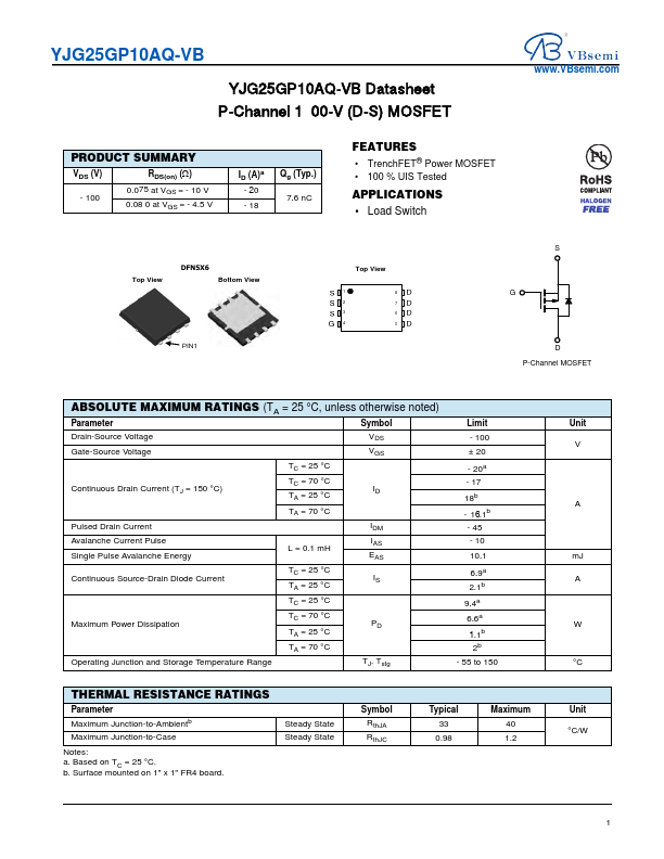
The following content is an automatically extracted verbatim text
from the original manufacturer datasheet and is provided for reference purposes only.
View original datasheet text
YJG25GP10AQ-VB
YJG25GP10AQ-VB Datasheet P-Channel 1 00-V (D-S) MOSFET
PRODUCT SUMMARY
VDS (V)
RDS(on) ()
- 100
0.075 at VGS = - 10 V 0.08 0 at VGS = - 4.5 V
ID (A)a - 20 - 18
Qg (Typ.) 7.6 nC
FEATURES • TrenchFET® Power MOSFET • 100 % UIS Tested
APPLICATIONS • Load Switch
www.VBsemi.com
Top View
DFN5X6 Bottom View
PIN1
Top View
1
8
2
7
3
6
4
5
S G
D P-Channel MOSFET
ABSOLUTE MAXIMUM RATINGS (TA = 25 °C, unless otherwise noted)
Parameter
Symbol
Drain-Source Voltage
VDS
Gate-Source Voltage
VGS
TC = 25 °C
Continuous Drain Current (TJ = 150 °C)
TC = 70 °C TA = 25 °C
ID
TA = 70 °C
Pulsed Drain Current
IDM
Avalanche Current Pulse Single Pulse Avalanche Energy
L = 0.