2N5114 Overview
Key Features
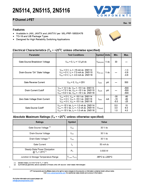
- Available in JAN, JANTX and JANTXV per MIL-PRF-19500/476
- TO-18 and UB Package Types
- Designed for High Reliability Switching Applications Rev. V2
| Part | 2N5114 |
|---|---|
| Description | P-Channel J-FET |
| Manufacturer | VPT Components |
| Size | 439.79 KB |
| Part Number | Manufacturer | Description |
|---|---|---|
| 2N5114 | Central Semiconductor | SILICON P-CHANNEL JFETS |
| 2N5114 | Microsemi | P-Channel J-FET |
| 2N5114 | InterFET | P-Channel JFET |
| 2N5114 | Micross | P-CHANNEL JFET |
| 2N5114 | Solitron Devices | P-CHANNEL JFETS |