VS3125
VS3125 is Quad Bus Switch with Individual Active Low Enables manufactured by Vaishali Semiconductor.
Description
The VS3125 contains a set of four high-speed, low-resistance bus switches. Each bus switch is individually controlled by TTL-patible, active-low control input (/x OE). The low ON resistance of VS3125 allows inputs to be connected to outputs without adding propagation delay and without generating additional signal noise. The VS3125 is function and pinout patible with QS3125. It enables 5V to 3.3V level translation when used with an external diode in the power supply line. In addition, the high off-isolation between switch terminals in the ‘disable’ mode, and the near-zero propagation delay in the ‘on’ state make the VS3V125 an ideal interface element for hot-swapping applications.
Features
- =
- =
- =
- =
- = Enhanced N-FET with no dc path to VCC or GND in normal operating signal voltage range. Low impedance bidirectional data flow Pin-patible with QS3125 & PI5C3125 switches Zero added ground bounce or signal noise TTL-patible control signals
- =
- =
- =
- =
- = Near-zero propagation delay Undershoot clamp diodes on all switch and control pins ESD rating >2000V (Human Body Model) or >200V (Machine Model) Latch-up current >100m A Available in 150-mil wide QSOP package
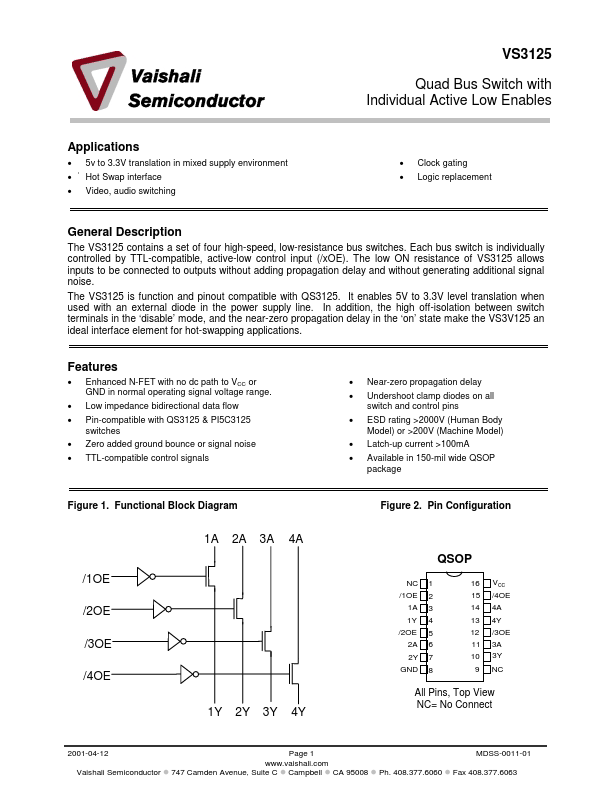
Figure 1. Functional Block Diagram
Figure 2. Pin Configuration
1A /1OE /2OE /3OE /4OE 1Y
2A
3A
4A QSOP
NC /1OE 1A 1Y /2OE 2A 2Y GND 1 2 3 4 5 6 7 8 16 15 14 13 12 11 10 9 VCC /4OE 4A 4Y /3OE 3A 3Y NC
2Y
3Y
4Y
All Pins, Top View NC= No Connect
2001-04-12 Vaishali Semiconductor
Page 1 .vaishali. 747 Camden Avenue, Suite C Campbell CA 95008
MDSS-0011-01 Ph. 408.377.6060 Fax 408.377.6063
Table 1. Pin Description
Name
1A
- 4A 1Y
- 4Y /1OE
- /4OE
I/O
I/O I/O I
Description
Data Input or Output Data Input or Output Bus Switch Enable
Table 2. Function Table /x OE
Path x A <-> x Y High...