50N02-09
FEATURES
PRODUCT SUMMARY
VDS (V)
20 r DS(on) (W)
0.0095 @ VGS = 10 V 0.017 @ VGS = 4.5 V
ID (A)a
20 15
Trench FETr Power MOSFET 175_C Junction Temperature PWM Optimized for High Efficiency 100% Rg Tested
APPLICATIONS
D High-Side Synchronous Buck DC/DC Conversion
- Desktop
- Server
..
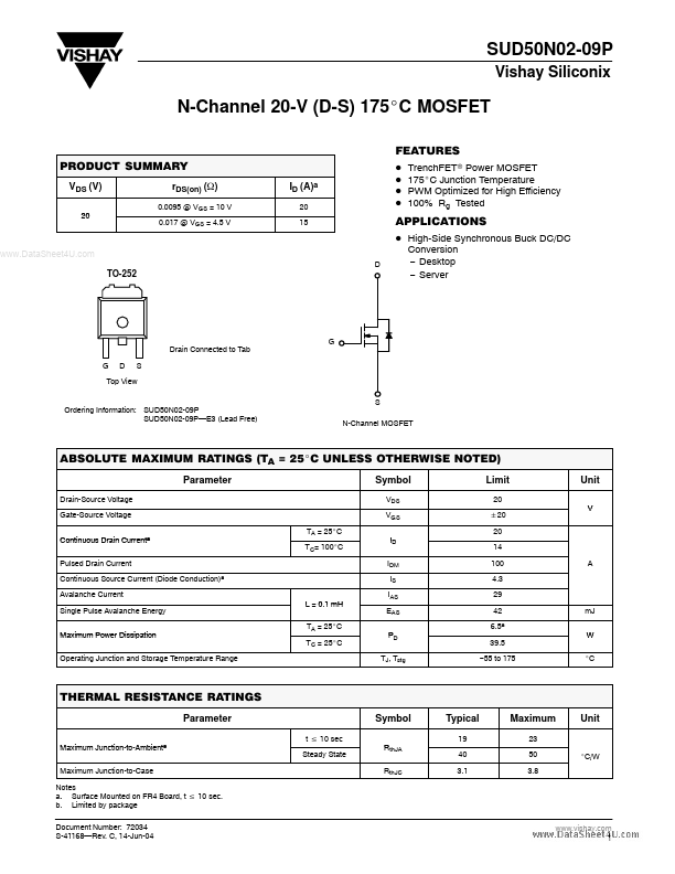
TO-252
Drain Connected to Tab G D S
Top View S N-Channel MOSFET
Ordering Information: SUD50N02-09P SUD50N02-09P- E3 (Lead Free)
ABSOLUTE MAXIMUM RATINGS (TA = 25_C UNLESS OTHERWISE NOTED)
Parameter
Drain-Source Voltage Gate-Source Voltage Continuous Drain Currenta Pulsed Drain Current Continuous Source Current (Diode Conduction)a Avalanche Current Single Pulse Avalanche Energy Maximum Power Dissipation Operating Junction and Storage Temperature Range L = 0.1 0 1 m H TA = 25_C TC = 25_C TA = 25_C TC= 100_C
Symbol
VDS VGS ID IDM IS IAS EAS PD TJ, Tstg
Limit
20 "20 20 14 100 4.3 29 42 6.5a 39.5
- 55 to 175
Unit
A m J W _C
THERMAL RESISTANCE RATINGS
Parameter
Maximum Junction...