IRFU320
IRFU320 is Power MOSFET manufactured by Vishay.
- Part of the IRFR320 comparator family.
- Part of the IRFR320 comparator family.
FEATURES
- Dynamic d V/dt rating
- Repetitive avalanche rated
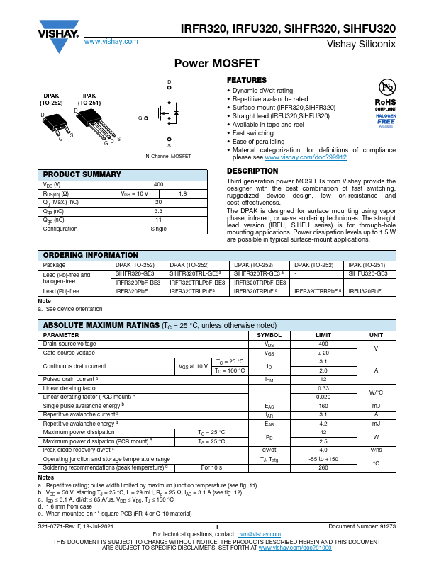
- Surface-mount (IRFR320,Si HFR320)
- Straight lead (IRFU320,Si HFU320)
- Available in tape and reel
- Fast switching
Available
- Ease of paralleling
- Material categorization: for definitions of pliance please see .vishay./doc?99912
DESCRIPTION
Third generation power MOSFETs from Vishay provide the designer with the best bination of fast switching, ruggedized device design, low on-resistance and cost-effectiveness.
The DPAK is designed for surface mounting using vapor phase, infrared, or wave soldering techniques. The straight lead version (IRFU, Si HFU series) is for through-hole mounting applications. Power dissipation levels up to 1.5 W are possible in typical surface-mount applications.
ORDERING INFORMATION
Package
DPAK (TO-252)
Lead (Pb)-free and halogen-free
Si HFR320-GE3 IRFR320Pb F-BE3
Lead (Pb)-free
IRFR320Pb F
Note a. See device orientation
DPAK (TO-252) Si HFR320TRL-GE3a IRFR320TRLPb F-BE3 IRFR320TRLPb Fa
DPAK (TO-252) Si HFR320TR-GE3 a IRFR320TRPb F-BE3 IRFR320TRPb F a
DPAK (TO-252)
- IPAK (TO-251) Si HFU320-GE3
IRFR320TRRPb F a IRFU320Pb F
ABSOLUTE MAXIMUM RATINGS (TC = 25 °C, unless otherwise noted)
PARAMETER
SYMBOL
Drain-source voltage Gate-source voltage
Continuous drain current
Pulsed drain current a Linear derating factor Linear derating factor (PCB mount) e Single pulse avalanche energy b Repetitive avalanche current a Repetitive avalanche energy a Maximum power dissipation Maximum power dissipation (PCB mount) e Peak diode recovery d V/dt c Operating junction and storage temperature range Soldering remendations (peak temperature) d
VGS at 10 V
TC = 25 °C TC = 100 °C
TC = 25 °C TA = 25 °C
For 10 s
VDS VGS ID IDM
EAS IAR EAR PD d V/dt TJ, Tstg
Notes a. Repetitive rating; pulse width limited by maximum junction temperature (see fig. 11) b. VDD = 50 V, starting TJ = 25 °C, L = 29 m H, Rg = 25 Ω, IAS = 3.1 A (see fig. 12) c. ISD ≤ 3.1 A, d I/dt ≤ 65 A/μs, VDD ≤ VDS, TJ ≤ 150 °C...