SI5402BDC Overview
Key Specifications
Package: SMD/SMT
Mount Type: Surface Mount
Pins: 8
Height: 1.0922 mm
Description
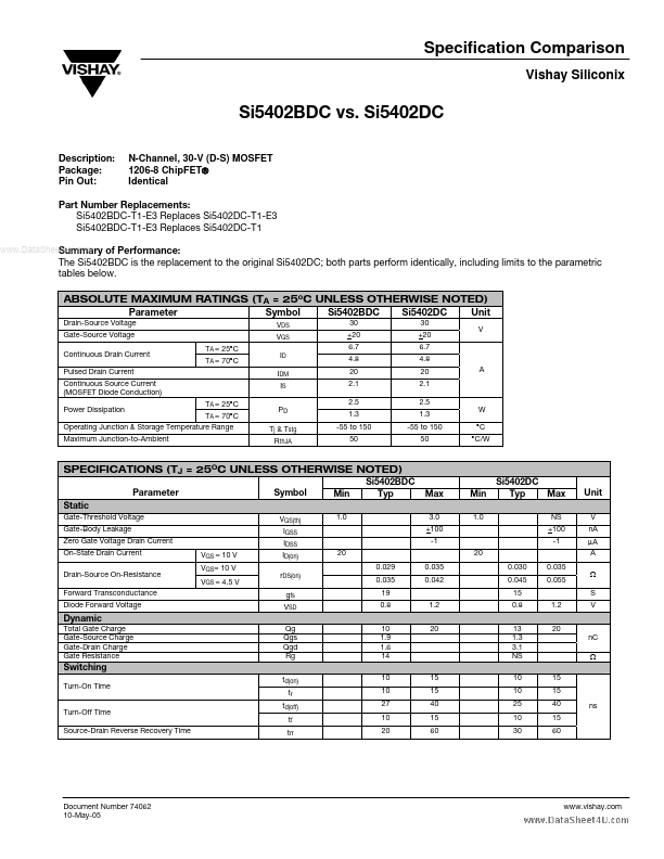
Package: Pin Out: N-Channel, 30-V (D-S) MOSFET 1206-8 ChipFET® Identical Part Number Replacements: Si5402BDC-T1-E3 Replaces Si5402DC-T1-E3 Si5402BDC-T1-E3 Replaces Si5402DC-T1 Summary of Performance: The Si5402BDC is the replacement to the original Si5402DC; both parts perform identically, including limits to the parametric tables below. Drain-Source Voltage Gate-Source Voltage Continuous Drain Current Pulsed Drain Current Continuous Source Current (MOSFET Diode Conduction) Power Dissipation TA = 25°C TA = 70°C Operating Junction & Storage Temperature Range Maximum Junction-to-Ambient TA = 25°C TA = 70°C VDS VGS ID IDM IS PD Tj & Tstg RthJA 30 +20 6.7 4.8 20 2.1 2.5 1.3 -55 to 150 50 30 +20 6.7 4.8 20 2.1 2.5 1.3 -55 to 150 50 W °C °C/W A V SPECIFICATIONS (TJ = 25OC UNLESS OTHERWISE NOTED) Parameter Static Gate-Threshold Voltage Gate-Body Leakage Zero Gate Voltage Drain Current On-State Drain Current Drain-Source On-Resistance Forward Transconductance Diode Forward Voltage VGS = 10 V VGS= 10 V VGS = 4.5 V VGS(th) IGSS IDSS ID(on) rDS(on) gfs VSD Qg Qgs Qgd Rg td(on) tr td(off) tf trr 20 0.029 0.035 19 0.8 10 1.9 1.6 14 10 10 27 10 20 1.2 20 0.035 0.042 1.0 3.0 +100 -1 20 0.030 0.045 15 0.8 13 1.3 3.1 NS 10 10 25 10 30 1.2 20 nC Ω 15 15 40 15 60 ns 0.035 0.055 1.0 NS +100 -1 V nA µA A Ω S V Symbol Min Si5402BDC Typ Max Min Si5402DC Typ Max Unit Dynamic Total Gate Charge Gate-Source Charge Gate-Drain Charge Gate Resistance Switching 15 15 40 15 60 Turn-On Time Turn-Off Time Source-Drain Reverse Recovery Time Document Number 74062 10-May-05.