SUM110N02-03P
FEATURES r DS(on) (W) ID (A)a
110a 110a
0.0032 @ VGS = 10 V 0.0052 @ VGS = 4.5 V
D Trench FETr Power MOSFET D 175_C Junction Temperature D Optimized for Low-Side Synchronous Rectifier
APPLICATIONS
D Synchronous Buck DC/DC Conversion
- Desktop
- Server D Load Switch
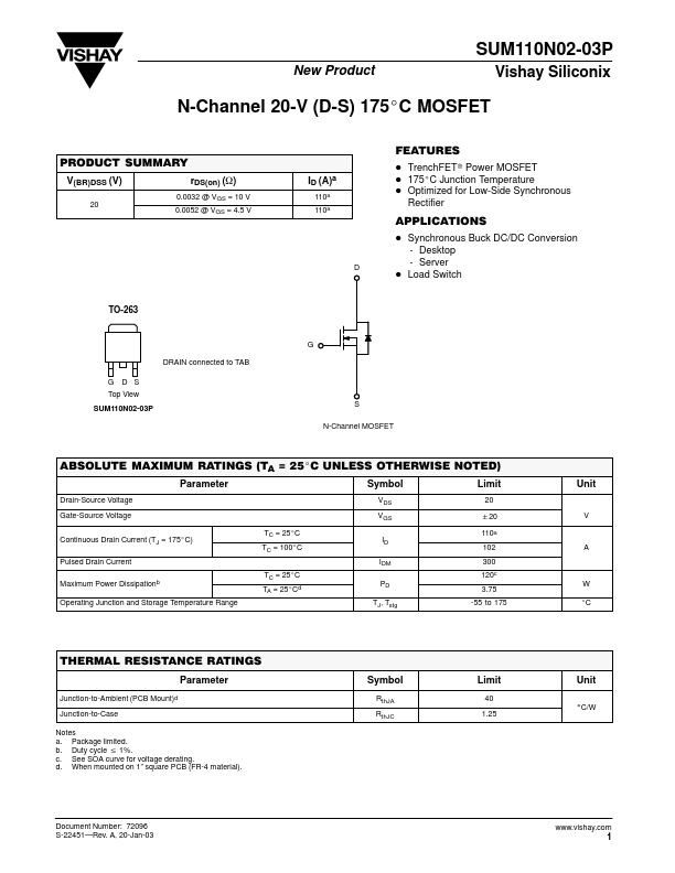
TO-263
G DRAIN connected to TAB G D S S N-Channel MOSFET
Top View SUM110N02-03P
ABSOLUTE MAXIMUM RATINGS (TA = 25_C UNLESS OTHERWISE NOTED)
Parameter
Drain-Source Voltage Gate-Source Voltage Continuous Drain Current (TJ = 175_C) Pulsed Drain Current Maximum Power Dissipationb Operating Junction and Storage Temperature Range TC = 25_C TA = 25_Cd TC = 25_C TC = 100_C
Symbol
VDS VGS ID IDM PD TJ, Tstg
Limit
20 "20 110a 102 300 120c 3.75 -55 to 175
Unit
W _C
THERMAL RESISTANCE RATINGS
Parameter
Junction-to-Ambient (PCB Junction-to-Case Notes a. Package limited. b. Duty cycle v 1%. c. See SOA curve for voltage derating. d. When mounted on 1” square PCB (FR-4 material). Mount)d
Symbol
Rth JA Rth JC
Limit
40...