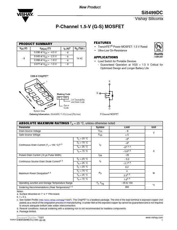
Si5499DC
Si5499DC is P-Channel 1.5-V MOSFET manufactured by Vishay.
FEATURES
- Trench FET® Power MOSFET: 1.5 V Rated
- Ultra-Low On-Resistance
Ro HS
APPLICATIONS
PLIANT
- Load Switch for Portable Devices
- Guaranteed Operation at VGS = 1.5 V Critical for Optimized Design and Longer Battery Life
1206-8 Chip FET®
D D D D S D D G
Marking Code BP XXX Lot Traceability and Date Code Part # Code
D P-Channel MOSFET
Bottom View Ordering Information: Si5499DC-T1-E3 (Lead (Pb)-free)
ABSOLUTE MAXIMUM RATINGS TA = 25 °C, unless otherwise noted
Parameter Drain-Source Voltage Gate-Source Voltage TC = 25 °C Continuous Drain Current (TJ = 150 °C)a, b TC = 70 °C TA = 25 °C TA = 70 °C Pulsed Drain Current (10 µs Pulse Width) Continuous Source-Drain Diode Currenta, b TC = 25 °C TA = 25 °C TC = 25 °C Maximum Power Dissipationa, b TC = 70 °C TA = 25 °C TA = 70 °C Operating Junction and Storage Temperature Range Soldering Remendations (Peak Temperature) c, d
Symbol VDS VGS
Limit -8 ±5
- 6e
- 6e
- 6a, b, e
- 5.6a, b
Unit V
IDM IS
- 25
- 5.2
- 2.1a, b 6.2 4 2.5a, b 1.6a, b
- 55 to 150 260 W
TJ, Tstg
°C
Notes: a. Surface Mounted on 1" x 1" FR4 board. b. t = 5 s. c. See Solder Profile (http://.vishay./ppg?73257). The Chip FET is a leadless package. The end of the lead terminal is exposed copper (not plated) as a result of the singulation process in manufacturing. A solder fillet at the exposed copper tip cannot be guaranteed and is not required to ensure adequate bottom side solder interconnection. d. Rework conditions: manual soldering with a soldering iron is not remended for leadless ponents. e. Package limited. Document Number: 73321 S-80193-Rev. B, 04-Feb-08 .vishay. 1
New Product
Vishay Siliconix
THERMAL RESISTANCE RATINGS
Parameter Maximum Junction-to-Ambient a,...