S886T
Features
Integrated gate protection diodes Low noise figure High gain Biasing network on chip
D Improved cross modulation at gain reduction D High AGC-range D SMD package
1 2
94 9279
13 579
94 9278
95 10831
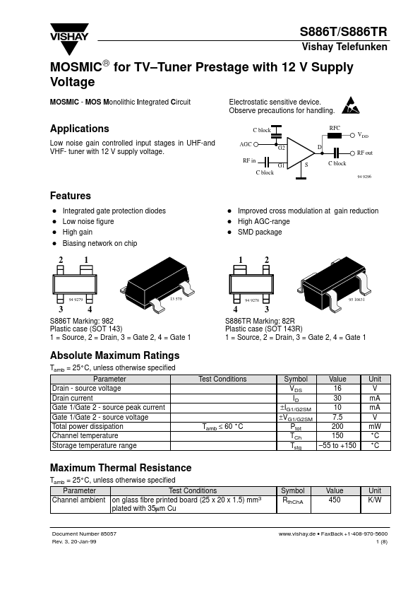
S886T Marking: 982 Plastic case (SOT 143) 1 = Source, 2 = Drain, 3 = Gate 2, 4 = Gate 1
S886TR Marking: 82R Plastic case (SOT 143R) 1 = Source, 2 = Drain, 3 = Gate 2, 4 = Gate 1
Absolute Maximum Ratings
Tamb = 25_C, unless otherwise specified Parameter Drain
- source voltage Drain current Gate 1/Gate 2
- source peak current Gate 1/Gate 2
- source voltage Total power dissipation Channel temperature Storage temperature range Test Conditions Symbol Value VDS 16 ID 30 ±IG1/G2SM 10 ±VG1/G2SM 7.5 Ptot 200 TCh 150 Tstg
- 55 to +150 Unit V m A m A V m W °C °C
Tamb ≤ 60 °C
Maximum Thermal Resistance
Tamb = 25_C, unless otherwise specified Parameter Test Conditions Channel ambient on glass fibre printed board (25 x 20 x 1.5) mm3 plated with 35mm Cu Symbol Rth...