APPLICATIONS
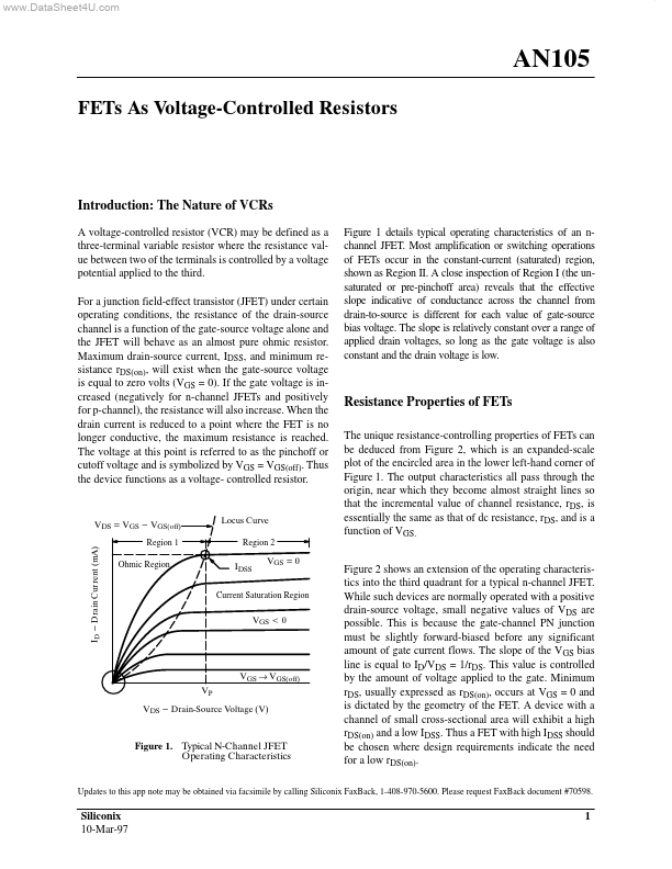
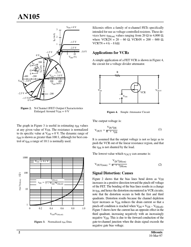
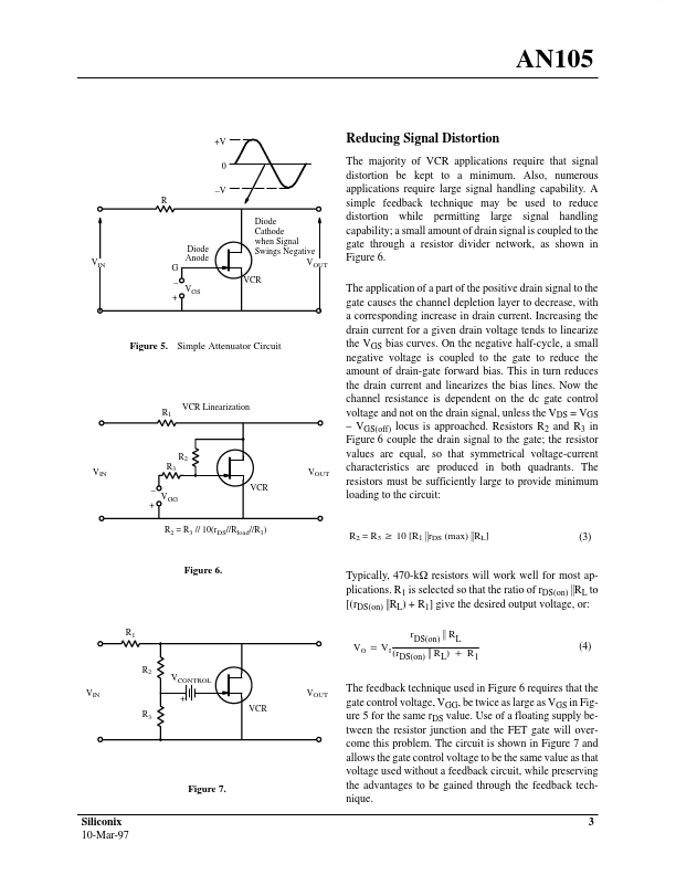
for VCRs A simple application of a FET VCR is shown in Figure 4, the circuit for a voltage divider attenuator. –2.5 V VGS = –3.0 V 200 400 VDS (mV) R VIN –2.5 V –1.5 V 0V –200 – + VCR VGS VOUT Figure 2. NĆChannel JFET Output Characteristics Enlarged Around VDS = 0 V Figure 4. Simple Attenuator Circuit The output voltage is: The graph in Figure 3 is useful in estimating rDS values at any given value of VGS. The resistance is normalized to its specific value at VGS = 0 V. The dynamic range of rDS is shown as greater than 100:1, although for best control of rDS a range of 10:1 is normally used. V IN rDS V OUT + R ) r (1) DS It is assumed that the output voltage is not so large as to push the VCR out of the linear resistance region, and that the rDS is not shunted by the load. The lowest value which vOUT can assume is: 1000 VDS ¬ 0.1 V V IN rDS(on) V OUT(min) + R ) r DS(on) (2) rDS /r DS(on) ( W ) 100 r DS(on) r DS ] 1 – V ńV GS GS(off) 10 Signal Distortion: Causes Figure 2 sh... Vishay