FEATURES
D Low Voltage Operation (1.8 V to 5.5 V) D Low On-Resistance - rDS(on): 1.2 W D Fast Switching - 14 ns D Low Charge Injection - QINJ: 1 pC D Low Power Consumption D TTL/CMOS Compatible D MSOP-8 Package BENEFITS D D D D Reduced Power Consumption Simple Logic Interface High Accuracy Reduce Board Space APPLICATIONS
D D D D D Cellular Phones Communication Systems Portable Test Equipment Battery Operated Systems Sample and Hold Circuits DESCRIPTION
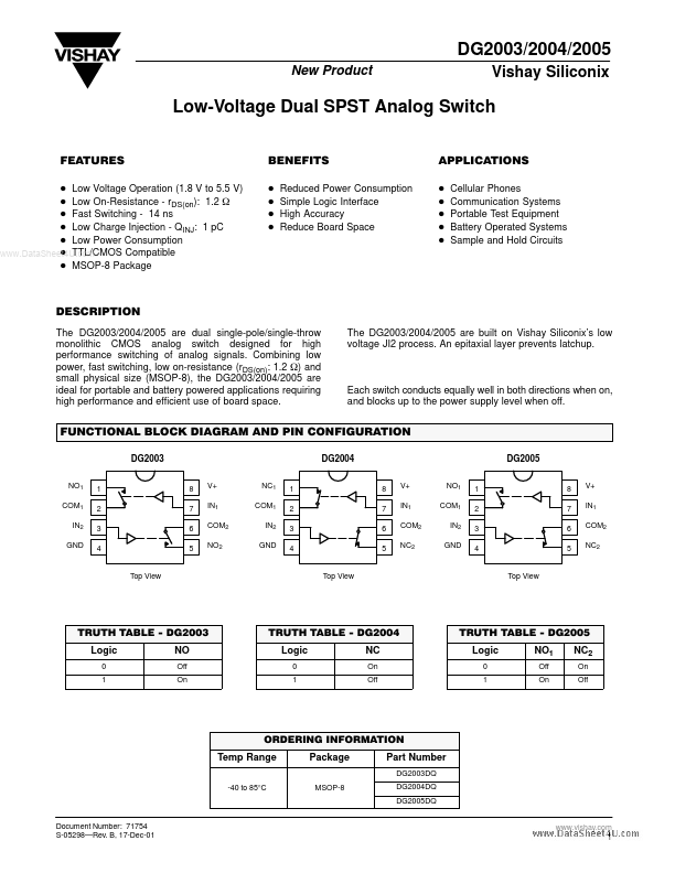
Combining low power, fast switching, low on-resistance (rDS(on): 1.2 W) and small physical size (MSOP-8), the DG2003/2004/2005 are ideal for portable and battery powered applications requiring high performance and efficient use of board space. An epitaxial layer prevents latchup. FUNCTIONAL BLOCK DIAGRAM AND PIN CONFIGURATION DG2003 NO1 COM1 IN2 GND V+ IN1 COM2 NO2 NC1 COM1 IN2 GND DG2004 V+ IN1 COM2 NC2 NO1 COM1 IN2 GND DG2005 V+ IN1 COM2 NC2 1 2 3 4 8 7 6 5 1 2 3 4 8 7 6 5 1 2 3 4 8 7 6 5 Top View Top View Top View TRUTH TABLE - DG2003... Vishay