FEATURES
D Low Voltage Operation (2.7 V to 3.3 V) D Low On-Resistance - rON: 0.85 W D 3 dB Loss @ 100 MHz D Fast Switching: tON = 40 ns tOFF = 35 ns D QFN-16 Package BENEFITS D D D D D Reduced Power Consumption High Accuracy Reduce Board Space TTL/1.8-V Logic Compatible High Bandwidth APPLICATIONS
D D D D D Cellular Phones Speaker Headset Switching Audio and Video Signal Routing PCMCIA Cards Battery Operated Systems DESCRIPTION
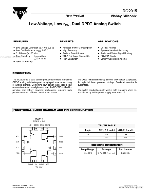
An epitaxial layer prevents latchup. Break-before-make is guaranteed. The switch conducts equally well in both directions when on, and blocks up to the power supply level when off. FUNCTIONAL BLOCK DIAGRAM AND PIN CONFIGURATION DG2015 QFN-16 (4 X 4) NC1 COM1 GND COM4 16 15 14 13 TRUTH TABLE Logic 0 12 11 10 9 NC4 NO4 NC1, 2, 3 and 4 ON OFF NO1, 2, 3 and 4 OFF ON NO1 INA NO2 NC2 1 2 3 4 1 ORDERING INFORMATION INB Temp Range NO3 -40 to 85°C Package 16-Pin QFN (4 x 4 mm) Part Number DG2015DN 5 COM2 6 V+ 7 8 COM3 NC3 Top View Document Number: 71971 S-03423—Rev. B, 0... Vishay