Si7390DP
Si7390DP is N-Channel MOSFET manufactured by Vishay.
FEATURES
- Halogen-free According to IEC 61249-2-21 Definition
- Extremely Low Qgd for Low Switching Losses
- Trench FET® Power MOSFET
- New Low Thermal Resistance Power PAK® Package with Low 1.07 mm Profile
- 100 % Rg Tested
- pliant to Ro HS Directive 2002/95/EC
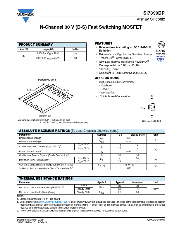
Power PAK SO-8
APPLICATIONS
- High-Side DC/DC Conversion
- Notebook
- Server
- Workstation
- Point-of-Load Conversion
6.15 mm
S 1 2 3 S S
5.15 mm
G 4
D 8 7 6 5 D D D
Bottom View Ordering Information: Si7390DP-T1-E3 (Lead (Pb)-free) Si7390DP-T1-GE3 (Lead (Pb)-free and Halogen-free)
S N-Channel MOSFET
ABSOLUTE MAXIMUM RATINGS (TA = 25 °C, unless otherwise noted)
Parameter Drain-Source Voltage Gate-Source Voltage Continuous Drain Current (TJ = 150 °C)a Pulsed Drain Current Continuous Source Current (Diode Conduction)a Maximum Power Dissipationa Operating Junction and Storage Temperature Range Soldering Remendations (Peak Temperature)b, c TA = 25 °C TA = 70 °C TA = 25 °C TA = 70 °C Symbol VDS VGS ID IDM IS PD TJ, Tstg 10 s Steady State 30 ± 20 9 7 ± 50 1.5 1.8 1.1
- 55 to 150 260 Unit V
15 12 4.1 5 3.2
W °C
THERMAL RESISTANCE RATINGS
Parameter Maximum Junction-to-Ambient (MOSFET)a Maximum Junction-to-Case (Drain) t ≤ 10 s Steady State Steady State Symbol Rth JA Rth JC Typical 20 53 2.1 Maximum 25 70 3.2 Unit °C/W
Notes: a. Surface mounted on 1” x 1” FR4 board. b. See solder profile (.vishay./ppg?73257). The Power PAK SO-8 is a leadless package. The end of the lead terminal is exposed copper (not plated) as a result of the singulation process in manufacturing. A solder fillet at the exposed copper tip cannot be guaranteed and is not required to ensure adequate bottom side solder interconnection. c. Rework conditions: manual soldering with a soldering iron is not remended for leadless ponents.
Document Number: 72214 S11-0212-Rev. E, 14-Feb-11
.vishay. 1
Vishay Siliconix
SPECIFICATIONS (TJ = 25 °C, unless otherwise noted)
Parameter Static Gate Threshold Voltage Gate-Body Leakage Zero...