Si7483ADP
Si7483ADP is P-Channel MOSFET manufactured by Vishay.
FEATURES
- Halogen-free According to IEC 61249-2-21 Available
- Trench FET® Power MOSFETS
- New Low Thermal Resistance Power PAK® Package with Low 1.07 mm Profile
- 100 % Rg tested
APPLICATIONS
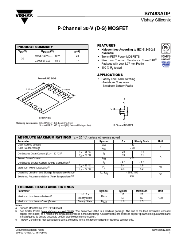
Power PAK SO-8
- Battery and Load Switching
- Notebook puters
- Notebook Battery Packs
5.15 mm
S 3 4 G
6.15 mm
S 1 2 S
D 8 7 6 5 D D D
Bottom View Ordering Information: Si7483ADP-T1-E3 (Lead (Pb)-free) Si7483ADP-T1-GE3 (Lead (Pb)-free and Halogen-free) D P-Channel MOSFET
ABSOLUTE MAXIMUM RATINGS TA = 25 °C, unless otherwise noted
Parameter Drain-Source Voltage Gate-Source Voltage Continuous Drain Current (TJ = 150 °C)a Pulsed Drain Current Continuous Source Current (Diode Conduction)a Maximum Power Dissipation a
Symbol VDS VGS TA = 25 °C TA = 70 °C ID IDM IS TA = 25 °C TA = 70 °C PD TJ, Tstg
10 s
- 24
- 19
- 4.5 5.4 3.4
Operating Junction and Storage Temperature Range Soldering Remendations (Peak Temperature)b,c
Steady State
- 30 ± 20
- 14
- 11
- 60
- 1.6 1.9 1.2
- 55 to 150 260
Unit V
W °C
THERMAL RESISTANCE RATINGS
Parameter Maximum Junction-to-Ambienta Maximum Junction-to-Case (Drain) t ≤ 10 s Steady State Steady State Symbol Rth JA Rth JC Typical 18 50 1.0 Maximum 23 65 1.5 Unit °C/W
Notes a. Surface Mounted on 1" x 1" FR4 board. b. See Solder Profile (.vishay./ppg?73257). The Power PAK SO-8 is a leadless package. The end of the lead terminal is exposed copper (not plated) as a result of the singulation process in manufacturing. A solder fillet at the exposed copper tip cannot be guaranteed and is not required to ensure adequate bottom side solder interconnection. c. Rework Conditions: manual soldering with a soldering iron is not remended for leadless ponents.
Document Number: 73025 S09-0270-Rev. C,...