Vishay TDA4173
TV Vertical Deflection Output Amplifier
| Part No. | TDA4173 |
|---|---|
| Datasheet | TDA4173 Download |
| Manufacturer |  Vishay |
| Description | TV Vertical Deflection Output Amplifier |
| Buy | Stock & Price |
FEATURES
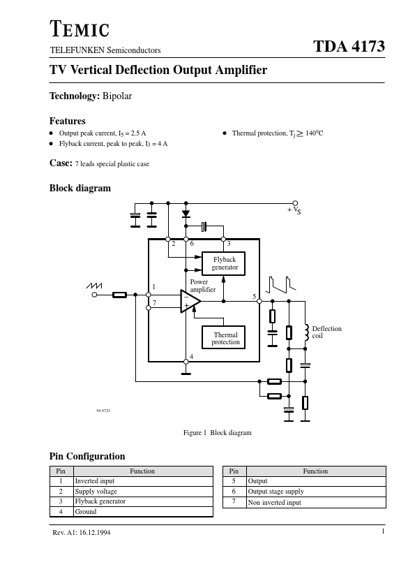
D Output peak current, I5 = 2.5 A D Flyback current, peak to peak, I3 = 4 A D Thermal protection, Tj 140°C Case: 7 leads special plastic case Block diagram + VS 2 6 3 Flyback generator 1 7 – + Power amplifier 5 Thermal protection 4 Deflection coil 94 8723 Figure 1 Block diagram Pin Configuration Pin 1 2 3 4 Function Inverted input Supply voltage Flyback generator Ground Pin 5 6 7 Function Output Output stage supply Non inverted input Rev. A1: 16.12.1994 1 TDA 4173ABSOLUTE MAXIMUM RATINGS
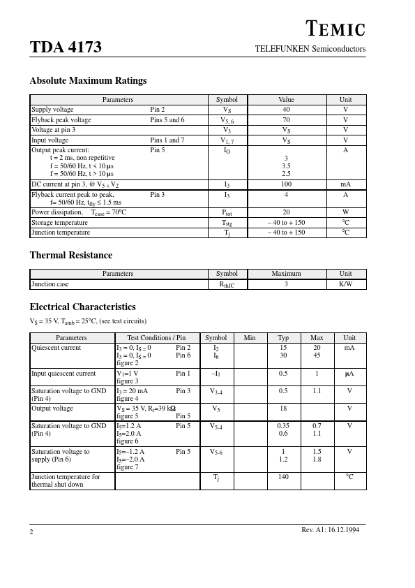
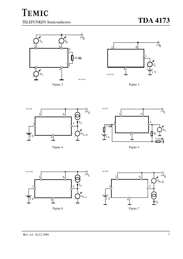
Parameters Supply voltage Flyback peak voltage Voltage at pin 3 Input voltage Output peak current: t = 2 ms, non repetitive f = 50/60 Hz, t < 10 ms f = 50/60 Hz, t > 10 ms DC current at pin 3, @ V5 < V2 Flyback current peak to peak, f= 50/60 Hz, tfly ≤ 1.5 ms Power dissipation, Tcase = 70°C Storage temperature Junction temperature Pin 2 Pins 5 and 6 Pins 1 and 7 Pin 5 Symbol VS V5, 6 V3 V1, 7 IO TELEFUNKEN Semiconductors Value 40 70 VS VS 3 3.5 2.5 Unit V V V V A Pin 3 I3 I3 Ptot Tstg Tj 100...