DTC114ESA
DTC114ESA is NPN DIGITAL TRANSISTOR manufactured by WEITRON.
Features
: without connecting external input resistors(see equivalent circuit). to allow negative biasing of the input.They also have the advantage device design easy.
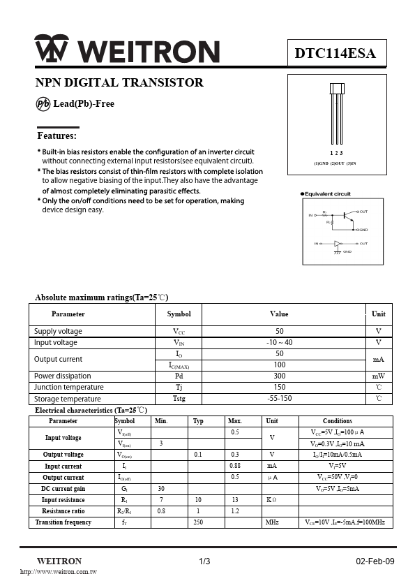
(1)GND (2)OUT (3)IN
Absolute maximum ratings(Ta=25℃)
Parameter
Symbol
Supply voltage Input voltage
Output current
Power dissipation Junction temperature Storage temperature
Electrical characteristics (Ta=25℃)
Parameter
Symbol
Input voltage
VI(off) VI(on)
Output voltage
VO(on)
Input current
Output current
IO(off)
DC current gain
Input resistance
R1
Resistance ratio
R2/R1
Transition frequency f T
VCC VIN IO IC(MAX) Pd Tj Tstg
Min.
Typ
3 0.1
30 7 10 0.8 1
Max. 0.5
0.3 0.88 0.5
13 1.2
Value
50 -10 ~ 40
50 100 300 150...