LD01N60
LD01N60 is Power FET manufactured by Wanlida.
FEATURES
Robust High Voltage Termination Avalanche Energy Specified Source-to-Drain Diode Recovery Time parable to a Discrete Fast Recovery Diode Diode is Characterized for Use in Bridge Circuits IDSS and VDS(on) Specified at Elevated Temperature
GENERAL DESCRIPTION
This high voltage MOSFET uses an advanced termination scheme to provide enhanced voltage-blocking capability without degrading performance over time. In addition, this advanced MOSFET is designed to withstand high energy in avalanche and mutation modes. The new energy efficient design also offers a drain-to-source diode with a fast recovery time. Designed for high voltage, high speed switching applications in power supplies, converters and PWM motor controls, these devices are particularly well suited for bridge circuits where diode speed and mutating safe operating areas are critical and offer additional and safety margin against unexpected voltage transients.
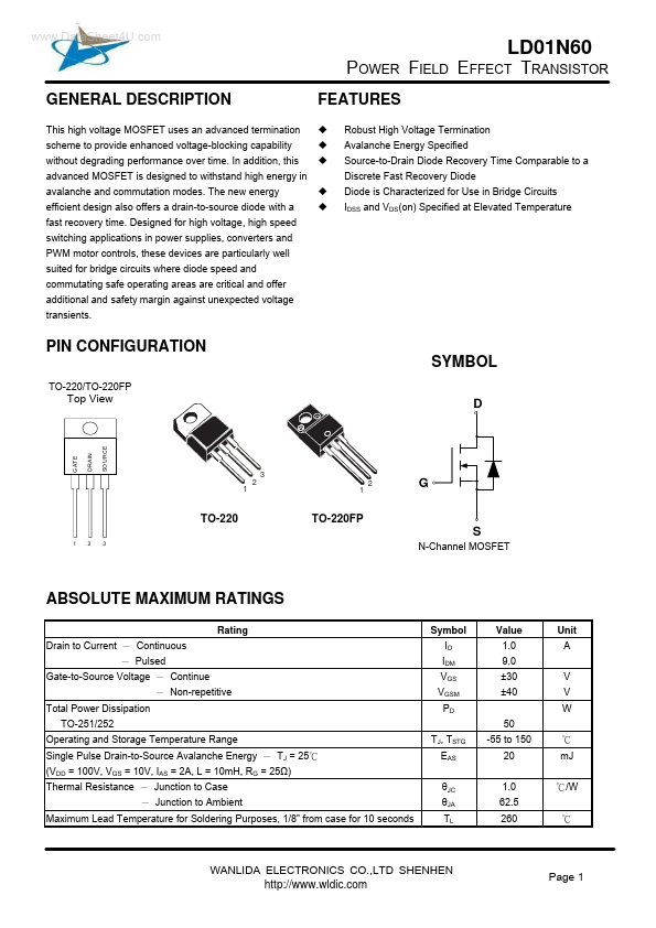
PIN CONFIGURATION SYMBOL
TO-220/TO-220FP
Top View
GATE
SOURCE
DRAIN
3 1 2
1 2
TO-220
1 2 3
TO-220FP
N-Channel MOSFET
ABSOLUTE MAXIMUM RATINGS
Rating Drain to Current - Continuous - Pulsed Gate-to-Source Voltage - Continue - Non-repetitive Total Power Dissipation TO-251/252 Operating and Storage Temperature Range Single Pulse Drain-to-Source Avalanche Energy - TJ = 25℃ (VDD = 100V, VGS = 10V, IAS = 2A, L = 10m H, RG = 25Ω) Thermal Resistance - Junction to Case - Junction to Ambient Maximum Lead Temperature for Soldering Purposes, 1/8” from case for 10 seconds θJC θJA TL 1.0 62.5 260 ℃ ℃/W TJ, TSTG EAS Symbol ID IDM VGS VGSM PD 50 -55 to 150 20 ℃ m J Value 1.0 9.0 ±30 ±40 V V W Unit A
WANLIDA ELECTRONICS CO.,LTD SHENZHEN http://.wldic.
Page 1
..
POWER FIELD EFFECT TRANSISTOR
ORDERING INFORMATION
Part Number LD01N60N251 LD01N60N252 LD01N60N92 LD01N60GN251- LD01N60GN252- LD01N60GN92-
- Note: G : Suffix for Pb Free Product Package TO-251 TO-252 TO-92 TO-251 TO-252 TO-92
ELECTRICAL CHARACTERISTICS
Unless...