WeEn Semiconductors WN3S20S100CB
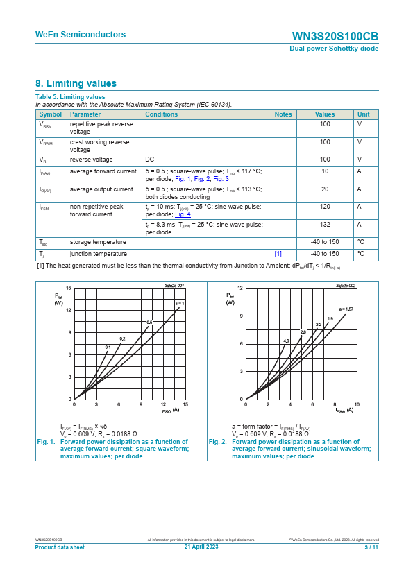
The heat generated must be less than the thermal conductivity from Junction to Ambient: dPtot/dTj < 1/Rth(j-a) Unit V V V A A A A °C °C Fig.| Part No. | WN3S20S100CB |
|---|---|
| Datasheet | WN3S20S100CB Download |
| Manufacturer |  WeEn Semiconductors |
| Description | Dual power Schottky diode |
| Buy | Stock & Price |
FEATURES AND BENEFITS
● Trench structure● High junction temperature up to 150 °C
● Low forward voltage drop, negligible switching losses
● High efficiency 3.
APPLICATIONS
● DC to DC converters● Freewheeling diode
● OR-ing diode
● Switched mode power supply rectifier 4. Quick reference data Table 1. Quick reference data Symbol Parameter Absolute maximum rating Conditions VRRM repetitive peak reverse voltage IF(AV) average forward current δ = 0.5 ; square-wave pulse; Tmb ≤ 117 °C; per diode; Fig. 1; Fig. 2; Fig. 3 IO(AV) average output current δ = 0.5 ; square-wave pulse; Tmb ≤ 113 °C; both diodes conducting Symbol Parameter Conditions Static characteristics VF forward voltage IF = 10 A; Tj = 25 °C; per diode; Fig. 6 IR reverse current VR = 100 V; Tj = 25 °C; per diode; Fig. 7; Fig. 8 Notes Notes Min - Values 100 10 20 Typ Max 0.90 1.00 2.5 15 Unit V A A Unit V μA WeEn Semiconductors 5. Pinning information Table 2. Pinning information Pin Symbol
DESCRIPTION
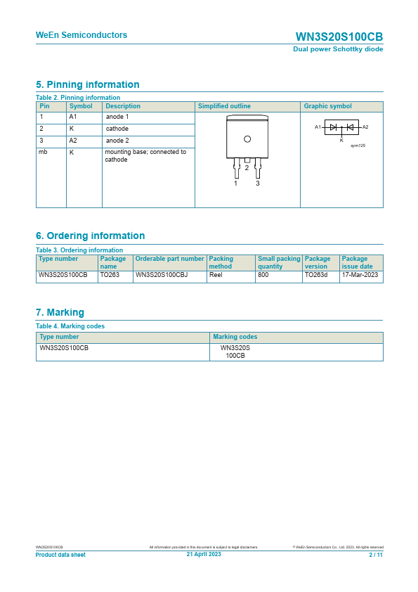
1 A1 anode 1 2 K cathode 3 A2 anode 2 mb K mounting base; connected to cathode Simplified outline 2 1 3 WN3S20S100CB Dual power Schottky diode Graphic symbol A1 A2 K sym125 6.