CG6258AM
Key Features
- Wide voltage range: 2.70V-3.30V
- Access Time: 70ns
- Ultra-low active power - Typical active current: 2.0mA @ f = 1 MHz * * * *
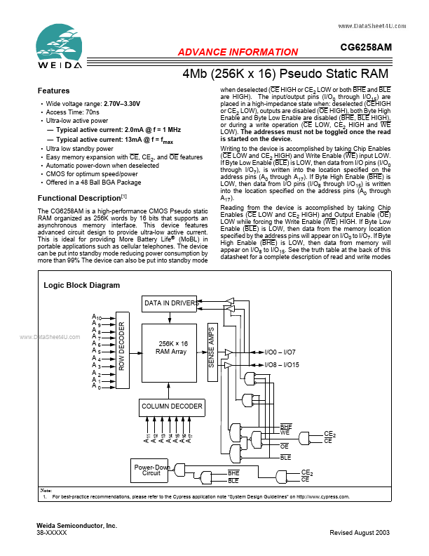
- - Typical active current: 13mA @ f = fmax Ultra low standby power Easy memory expansion with CE, CE2, and OE features Automatic power-down when deselected CMOS for optimum speed/power Offered in a 48 Ball BGA Package when deselected (CE HIGH or CE2 LOW or both BHE and BLE are HIGH). The input/output pins (I/O0 through I/O15) are placed in a high-impedance state when: deselected (CEHIGH or CE2 LOW), outputs are disabled (OE HIGH), both Byte High Enable and Byte Low Enable are disabled (BHE, BLE HIGH), or during a write operation (CE LOW, CE2 HIGH and WE LOW). The addresses must not be toggled once the read is started on the device. Writing to the device is accomplished by taking Chip Enables (CE LOW and CE2 HIGH) and Write Enable (WE) input LOW. If Byte Low Enable (BLE) is LOW, then data from I/O pins (I/O0 through I/O7), is written into the location specified on the address pins (A0 through A17). If Byte High Enable (BHE) is LOW, then data from I/O pins (I/O8 through I/O15) is written into the location specified on the address pins (A0 through A17). Reading from the device is accomplished by taking Chip Enables (CE LOW and CE2 HIGH) and Output Enable (OE) LOW while forcing the Write Enable (WE) HIGH. If Byte Low Enable (BLE) is LOW, then data from the memory location specified by the address pins will appear on I/O0 to I/O7. If Byte High Enable (BHE) is LOW, then data from memory will appear on I/O8 to I/O15. See the truth table at the back of this datasheet for a complete description of read and write modes Functional Description[1] The CG6258AM is a high-performance CMOS Pseudo static RAM organized as 256K words by 16 bits that supports an asynchronous memory interface. This device features advanced circuit design to provide ultra-low active current. This is ideal for providing More Battery Life® (MoBL) in portable applications such as cellular telephones. The device can be put into standby mode reducing power consumption by more than 99% The device can also be put into standby mode Logic Block Diagram