WCFS0808V1E
Features
- Single 3.3V power supply
- Ideal for low-voltage cache memory applications
- High speed
- 12/15 ns
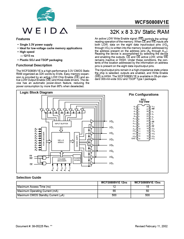
- Plastic SOJ and TSOP packaging An active LOW Write Enable signal (WE) controls the writing/ reading operation of the memory. When CE and WE inputs are both LOW, data on the eight data input/output pins (I/O0 through I/O7) is written into the memory location addressed by the address present on the address pins (A0 through A14). Reading the device is acplished by selecting the device and enabling the outputs, CE and OE active LOW, while WE remains inactive or HIGH. Under these conditions, the contents of the location addressed by the information on address pins is present on the eight data input/output pins. The input/output pins remain in a high-impedance state unless the chip is selected, outputs are enabled, and Write Enable (WE) is HIGH. The WCFS0808V1E is available in 28-pin standard 300-mil-wide SOJ and TSOP Type I packages.
Functional Description
The WCFS0808V1E is a...