MUN5133DW
MUN5111DW Series Dual Bias Resistor Transistor PNP Silicon
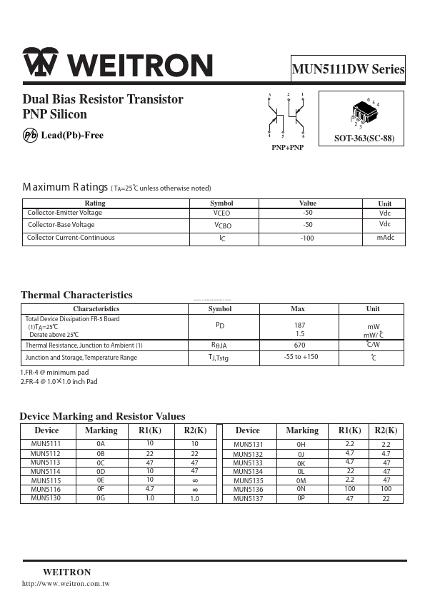
3 2 1
6 5
4 5 6
SOT-363(SC-88)
PNP+PNP
M aximum R atings ( TA=25 C unless otherwise noted)
Rating Collector-Emitter Voltage Collector-Base Voltage Collector Current-Continuous Symbol VCEO VCBO IC Value -50 -50 -100 Unit Vdc Vdc m Adc
Thermal Characteristics
Characteristics
Total Device Dissipation FR-5 Board (1)TA=25 C Derate above 25 C Thermal Resistance, Junction to Ambient (1) Junction and Storage, Temperature Range
..
Symbol PD R θJA TJ,Tstg
Max 187 1.5 670 -55 to +150
Unit m W m W/ C C/W C
1.FR-4 @ minimum pad 2.FR-4 @ 1.0 l 1.0 inch Pad l
Device Marking and Resistor Values
Device
MUN5111 MUN5112 MUN5113 MUN5114 MUN5115 MUN5116 MUN5130
Marking
0A 0B 0C 0D 0E 0F 0G
R1(K)
10 22 47 10 10 4.7 1.0
R2(K)
10 22 47 47 8 8
Device
MUN5131 MUN5132 MUN5133 MUN5134 MUN5135 MUN5136 MUN5137
Marking
0H 0J 0K 0L 0M 0N 0P
R1(K)
2.2 4.7 4.7 22 2.2 100 47
R2(K)
2.2 4.7 47 47 47 100 22
WE ITR O N...