Datasheet Summary
偉詮電子股份有限公司 Weltrend Semiconductor, Inc.
`
PC POWER SUPPLY SUPERVISOR
Data Sheet
REV. 1.01 November 30, 2010
The information in this document is subject to change without notice. ©Weltrend Semiconductor, Inc. All Rights Reserved. 新竹市科學工業園區工業東九路24號2樓 2F, No. 24, Industry E. 9th RD., Science-Based Industrial Park, Hsin-Chu, Taiwan TEL:886-3-5780241 FAX:886-3-5794278.5770419
Rev. 1.01
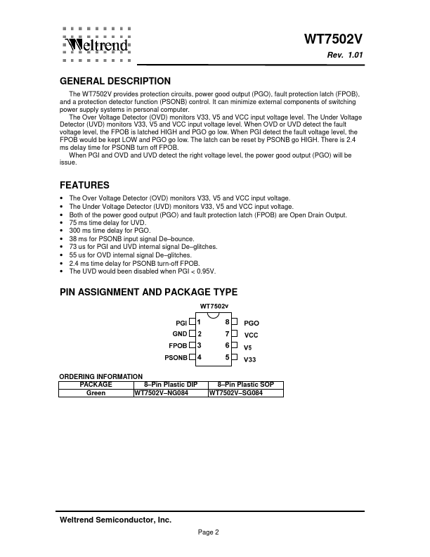
GENERAL DESCRIPTION
The WT7502V provides protection circuits, power good output (PGO), fault protection latch (FPOB), and a protection detector function (PSONB) control. It can minimize external ponents of switching power supply systems in personal puter.
The Over Voltage Detector (OVD)...