DESCRIPTION
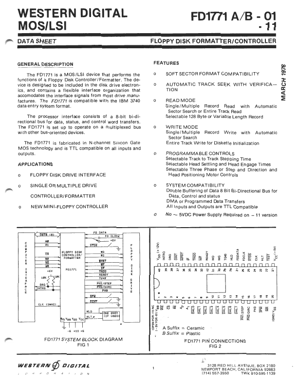
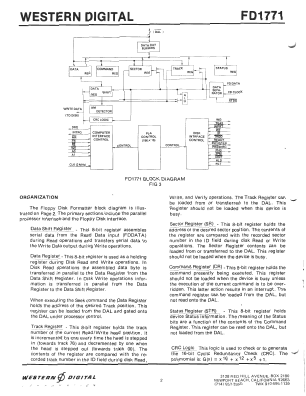
1.1 FD1771 - Flexible Drive Interface (Refer to Figure 1-1 FD1771 Block Diagram) Each data cell is defined by clock pulses. A pulse write head over the desired track. The Address Marks for Index,1 D, and Data are identified PH2, and PH3 for 3 phase stepping motors or by sending a level over the PH2 line and pulses over the PH 1 lines to deter- by a particular pattern not repeated in the remainder of the mine direction and stepping rate tor step-direction motors. ID field or Data field. This is accomplished by reading patterns The particular motor interface is chosen by hardwiring the ex- that are recorded with missing clock bits (logic 0) as shown ternal pin, 3PM. below: ALL REFERENCE TO FD1171 DENOTESFD1771-01 VERSION IC I0 M P U T E R I N T E R F A C E ,. nnA. (8) AO A1 B RE ~ Q'R +5V o{10K rL 10K (> ?ORO INTRO●- ClK (2 MHz) FLOPPY DISK CONTROllERI FORMATTER F01n1 FOOATA ~CLOCK ..., +5V -JrTm --~ WD WG WI'RT WI! TP TftCm READY TG43 PHlISTEP PH2/0lRC PH3 R "~-~ i5i'NT --~... Western Digital