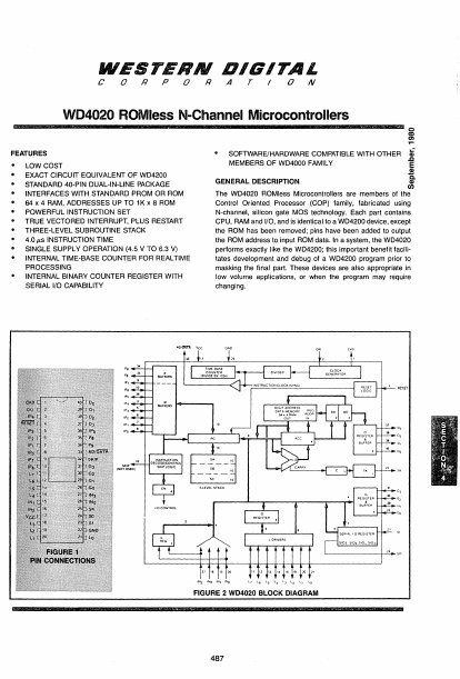
Description
System oscillalor output System oscillalor inpul 8 bidirectional ROM address and dala ports Syslem reset Input 8 bidirectional I/O ports with TRI-STATE® 4 general purpose Inputs Power supply Ground Serial input (or counter input) Serial output (or general purpose output) Logic-controlled clock (or general purpose output) 4 bidirectional I/O ports Instruction skip output Address out/data In flag 2 ROM address outputs 4 general purpose outputs 488 Voltage at Any Pin Relative to GND: Ambient Operating Temperature WD4020A,B WD4020AE, BE: Ambient Storage Temperature Lead Temperature (Soldering, 10 seconds) Power Dissipation -0.5V to + 7V O°C to + 70'C - 40°C to +85'C - 65'C to + 150'C 300'C 0.75 Watt at 25'C 0.4 Watt at 70'C DC Parameter Operating Voltage (Vee) Operating Supply Current Conditions Vee = 5V, TA = 25'C (all inputs and outputs open) Min Max Units 4.5 6.3 V 30 rnA Input Voltage Levels CKI Input Levels Logic High (VIH) Logic Low (V IU rlESET Input Levels Logic High Logic Low RESET Hysteresis SO Input Level (Test mode) All Other Inputs Logic High Logic High Logic Low Vee = max Vee = 5V '" 5% 2.0 0.7 Vee 1.0 2.0 3.0 2.0 V 0.4 V V 0.6 V V 3.0 V V V 0.8 V Output Voltage Levels (Note 2) TIL Operation Logic High (VO H) Logic Low (VOU CMOS Operation Logic High (VOH) Logic Low (Vall ')utput Current Levels LED Direct Drive Output Logic High (lOH) TRI-STATE'" Output Leakage Current Vee = 5V '" 5% IOH = 100!-,A IOl = -1.6mA IOH = 10fLA IOl = -10!-,A Vee = 6V VOH = 2.0V 2.4 Vee - 1 V 0.4 V V 0.2 V 2.5 14 rnA -10 +10 fLA 489 AC Parameter Conditions Min Max Units Instruction Cycle Time-tc CKI Using Crystal Input Frequency-II Duty Cycle (Note 2) ligure 3a +16 mode figure 3a 4 10 P.s 1.6 4 MHz 30 55 % INPUTS: INrINo. L7-Lo tSETUP tHOLO SI.IP 7-IP o tSETUP tHOLO 1.7 P.s 100 ns 0.3 p.s 100 ns OUTPUTS: COP TO CMOS PROPAGATION DELAY SK as a Logic-Controlled Clock tpOl tpoo SO.
Key Features
- IP7 --RESET Lo
- IN3 VCC GND SI SO SK Go