EDI8F32128C
EDI8F32128C is 128KX32 STATIC RAM CMOS manufactured by White Electronic Designs Corporation.
FEATURES
128Kx32 bit CMOS Static Random Access Memory
..
DESCRIPTION
The EDI8F32128C is a high speed 4Mb Static RAM module organized as 128K words by 32 bits. This module is constructed from four 128Kx8 Static RAMs in SOJ packages on an epoxy laminate (FR4) board. Four chip enables (E0#
- E3#) are used to independently enable the four bytes. Reading or writing can be executed on individual bytes or any bination of multiple bytes through proper use of selects. The EDI8F32128C is offered in 64 pin ZIP/SIMM package which enables eight megabits of memory to be placed in less than 1.4 square inches of board space. All inputs and outputs are TTL patible and operate from a single 5V supply. Fully asynchronous circuitry requires no clocks or refreshing for operation and provides equal access and cycle times for ease of use. The ZIP and SIMM modules contain two pins, PD1 and PD2, which are used to identify module memory density in applications where alternate modules can be interchanged.
Access Times: 15, 20, and 25ns Individual Byte Selects Fully Static, No Clocks TTL patible I/O Single +5V (±10%) Supply Operation High Density Package with JEDEC Standard Pinouts 64 Pin ZIP, No. 85
- Height: 13.97 (0.550") 64 Lead SIMM, No. 333
- Height: 15.62 (0.615") mon Data Inputs and Outputs
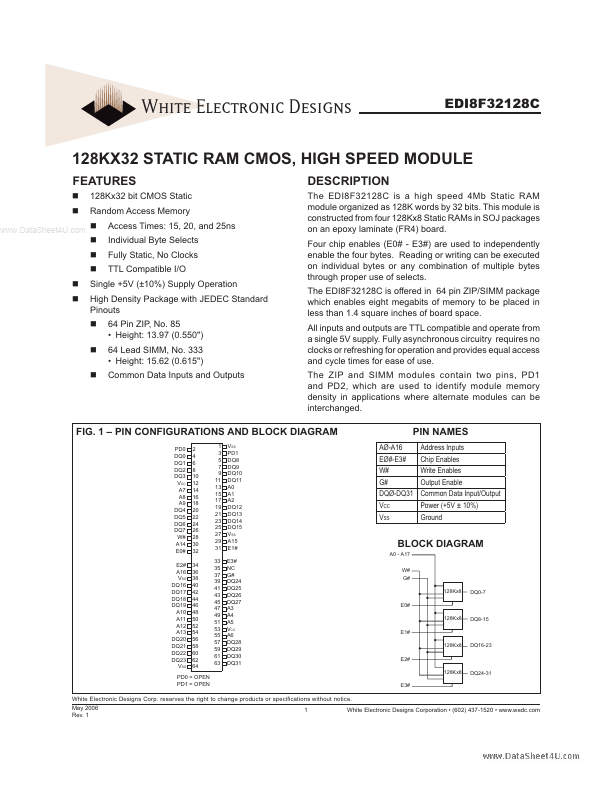
FIG. 1
- PIN CONFIGURATIONS AND BLOCK DIAGRAM
PD0 DQ0 DQ1 DQ2 DQ3 VCC A7 A8 A9 DQ4 DQ5 DQ6 DQ7 W# A14 E0# E2# A16 VSS DQ16 DQ17 DQ18 DQ19 A10 A11 A12 A13 DQ20 DQ21 DQ22 DQ23 VSS 2 4 6 8 10 12 14 16 18 20 22 24 26 28 30 32 34 36 38 40 42 44 46 48 50 52 54 56 58 60 62 64 1 3 5 7 9 11 13 15 17 19 21 23 25 27 29 31 33 35 37 39 41 43 45 47 49 51 53 55 57 59 61 63 VSS PD1 DQ8 DQ9 DQ10 DQ11 A0 A1 A2 DQ12 DQ13 DQ14 DQ15 VSS A15 E1# E3# NC G# DQ24 DQ25 DQ26 DQ27 A3 A4 A5 VCC A6 DQ28 DQ29 DQ30 DQ31
PIN NAMES
AØ-A16 EØ#-E3# W# G# DQØ-DQ31 VCC VSS Address Inputs Chip Enables Write Enables Output Enable mon Data Input/Output Power (+5V ± 10%) Ground
BLOCK DIAGRAM
A0
- A17 W# G# 128Kx8 E0# 128Kx8 E1# 128Kx8...