WS512K16-xxx
WS512K16-xxx is 512Kx16 SRAM MODULE manufactured by White Electronic Designs Corporation.
Features
Access Times 17, 20, 25, 35ns MIL-STD-883 pliant Devices Available Packaging
- 44 pin Ceramic SOJ (Package 102)
- 44 lead Ceramic Flatpack (Package 209) Organized as two banks of 256Kx16 Data Byte Control: Lower Byte (LB#) = I/O1-8 Upper Byte (UB#) = I/O9-16
ADVANCED-
Data I/O patible with 3.3V devices 2V Minimum Data Retention for battery back up operation mercial, Industrial and Military Temperature Range 5 Volt Power Supply (3.3V parts also available) Low Power CMOS TTL patible Inputs and Outputs
- This product is under development, is not qualified or characterized and is subject to change or cancellation without notice.
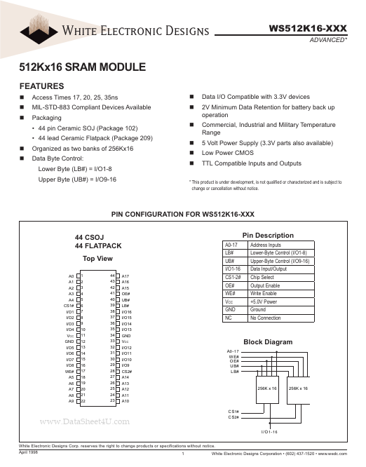
PIN CONFIGURATION FOR WS512K16-XXX 44 CSOJ 44 FLATPACK Top View
A0 A1 A2 A3 A4 CS1# I/O1 I/O2 I/O3 I/O4 VCC GND I/O5 I/O6 I/O7 I/O8 WE# A5 A6 A7 A8 A9
Pin Description
A0-17 LB# UB# I/O1-16 CS1-2# OE# WE# VCC GND NC Address Inputs Lower-Byte Control (I/O1-8) Upper-Byte Control (I/O9-16) Data Input/Output Chip Select Output Enable Write Enable +5.0V Power Ground No Connection
1 2 3 4 5 6 7 8 9 10 11 12 13 14 15 16 17 18 19 20 21 22
44 43 42 41 40 39 38 37 36 35 34 33 32 31 30 29 28 27 26 25 24 23
A17 A16 A15 OE# UB# LB# I/O16 I/O15 I/O14 I/O13 GND VCC I/O12 I/O11 I/O10 I/O9 CS2# A14 A13 A12 A11 A10
Block Diagram
A0
- 1 7 W E# O E# U B# L B#
256K x 16
256K x 16
..
White Electronic Designs Corp. reserves the right to change products or specifications without notice. April 1998 1
C S1# C S2#
I/O1-16
White Electronic Designs Corporation
- (602) 437-1520
- .wedc.
White Electronic Designs
TRUTH TABLE
CS1# H L H L H H L H L CS2# H H L H L L H L H L H WE# X H X H OE# X H X L LB# X X H L H L L H L UB# X X Output Disable H H L L H L L Read Data Out High Z Data Out Data In High Z Data In High Z Mode Not Select Data I/O I/O1-8
ADVANCED...