EDI7F328XDNSN Description
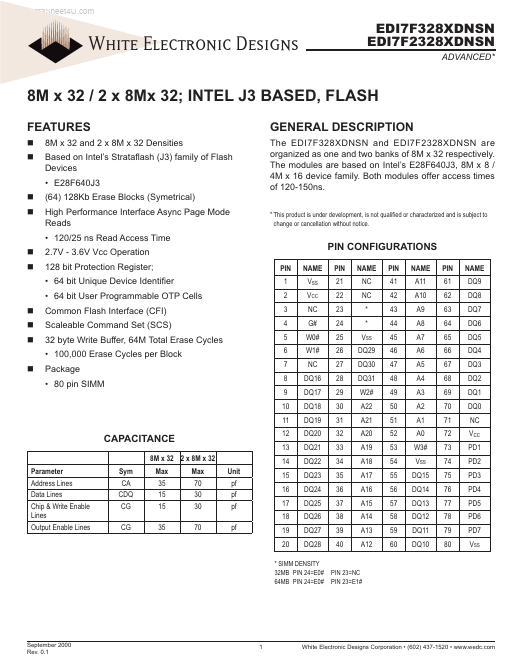
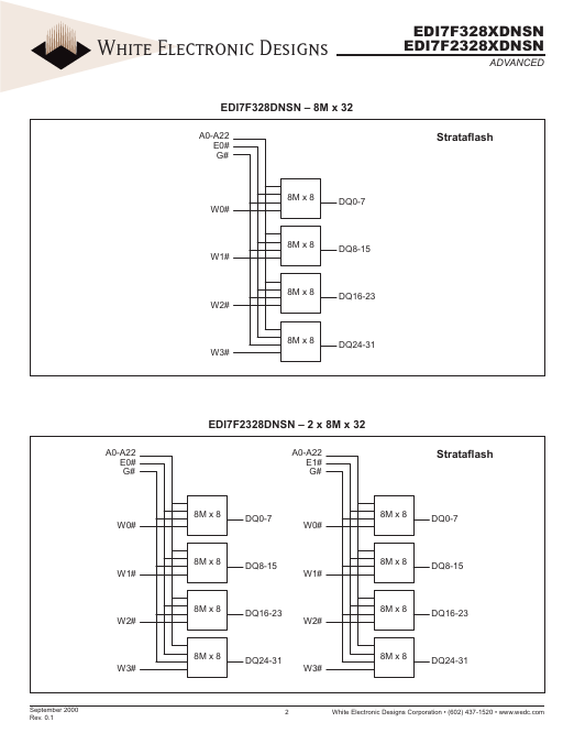
The EDI7F328XDNSN and EDI7F2328XDNSN are organized as one and two banks of 8M x 32 respectively. The modules are based on Intel’s E28F640J3, 8M x 8 / 4M x 16 device family. Both modules offer access times of 120-150ns.
EDI7F328XDNSN Key Features
- E28F640J3 (64) 128Kb Erase Blocks (Symetrical) High Performance Interface Async Page Mode Reads
- 120/25 ns Read Access Time 2.7V
- 3.6V Vcc Operation 128 bit Protection Register
- 64 bit Unique Device Identifier
- 64 bit User Programmable OTP Cells mon Flash Interface (CFI) Scaleable mand Set (SCS) 32 byte Write Buffer, 64M Total Er
- 100,000 Erase Cycles per Block Package
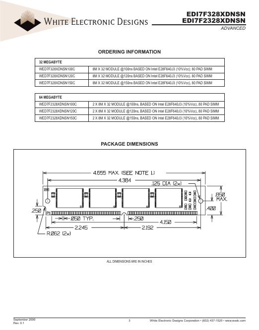
- 80 pin SIMM
- This product is under development, is not qualified or characterized and is subject to change or cancellation without not