Datasheet4U Logo Datasheet4U.com

WED2DG472512V-D2 - DUAL KEY DIMM

General Description

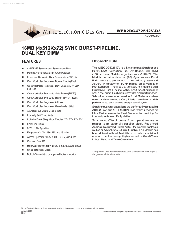
The WED2DG472512V is a Synchronous/Synchronous Burst SRAM, 84 position Dual Key; Double High DIMM (168 contacts) Module, organized as 4x512Kx72.

Key Features

  • 4x512Kx72 Synchronous, Synchronous Burst Pipeline Architecture; Single Cycle Deselect Linear and Sequential Burst Support via MODE pin Clock Controlled Registered Module Enable (EM#) Clock Controlled Registered Bank Enables (E1#, E2#, E3#, E4#) Clock Controlled Byte Write Mode Enable (BWE#) Clock Controlled Byte Write Enables (BW1# - BW8#) Clock Controlled Registered Address Clock Controlled Registered Global Write (GW#) Asynchronous Output Enable (G#) Internally Self-Timed Write Individual Bank.

📥 Download Datasheet

Datasheet Details

Part number WED2DG472512V-D2
Manufacturer White Electronic
File Size 207.33 KB
Description DUAL KEY DIMM
Datasheet download datasheet WED2DG472512V-D2 Datasheet

Full PDF Text Transcription (Reference)

The following content is an automatically extracted verbatim text from the original manufacturer datasheet and is provided for reference purposes only.

View original datasheet text
www.DataSheet4U.com White Electronic Designs WED2DG472512V-D2 ADVANCED* 16MB (4x512Kx72) SYNC BURST-PIPELINE, DUAL KEY DIMM FEATURES 4x512Kx72 Synchronous, Synchronous Burst Pipeline Architecture; Single Cycle Deselect Linear and Sequential Burst Support via MODE pin Clock Controlled Registered Module Enable (EM#) Clock Controlled Registered Bank Enables (E1#, E2#, E3#, E4#) Clock Controlled Byte Write Mode Enable (BWE#) Clock Controlled Byte Write Enables (BW1# - BW8#) Clock Controlled Registered Address Clock Controlled Registered Global Write (GW#) Asynchronous Output Enable (G#) Internally Self-Timed Write Individual Bank Sleep Mode Enables (ZZ1, ZZ2, ZZ3, ZZ4) Gold Lead Finish 3.3V ± 10% Operation Frequency(s): 200, 166, 150, and 133MHz Access Speed(s): tKHQV = 3.0, 3.5, 3.