WF2M32-XXX5
WF2M32-XXX5 is 2Mx32 5V Flash Module manufactured by White Electronic.
FEATURES
Access Time of 90, 120, 150ns Packaging:
- 66 pin, PGA Type, 1.185" square, Hermetic Ceramic HIP (Package 401).
- 68 lead, Hermetic CQFP (G2U), 22.4mm (0.880") square (Package 510) 3.56mm (0.140") height. Designed to fit JEDEC 68 lead 0.990" CQFJ footprint (FIGURE 3) Sector Architecture
- 32 equal size sectors of 64KBytes per each 2Mx8 chip
- Any bination of sectors can be erased. Also supports full chip erase. Minimum 100,000 Write/Erase Cycles Minimum Organized as 2Mx32
WF2M32-XXX5 mercial, Industrial, and Military Temperature Ranges 5 Volt Read and Write. 5V ± 10% Supply. Low Power CMOS Data# Polling and Toggle Bit feature for detection of program or erase cycle pletion. Supports reading or programming data to a sector not being erased. RESET# pin resets internal state machine to the read mode. Built in Decoupling Caps and Multiple Ground Pins for Low Noise Operation, Separate Power and Ground Planes to improve noise immunity
- This product is subject to change without notice. Note: For programming information refer to Flash Programming 16M5 Application Note.
..
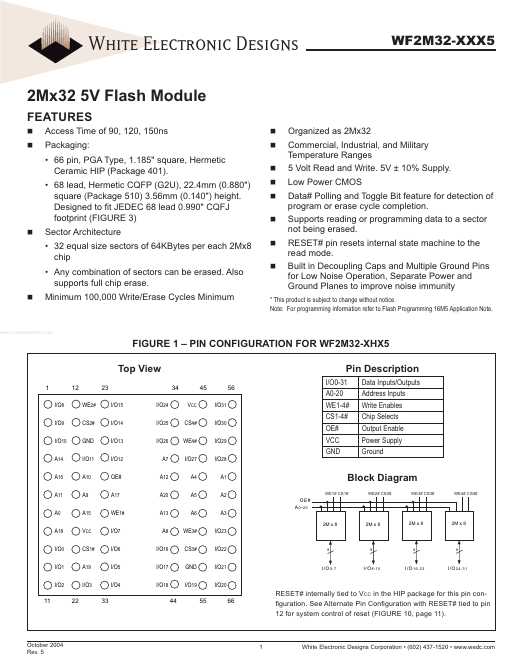
FIGURE 1
- PIN CONFIGURATION FOR WF2M32-XHX5 Top View
1 I/O8 I/O9 I/O10 A14 A16 A11 A0 A18 I/O0 I/O1 I/O2 11 22 12 WE2# CS2# GND I/O11 A10 A9 A15 VCC CS1# A19 I/O3 33 23 I/O15 I/O14 I/O13 I/O12 OE# A17 WE1# I/O7 I/O6 I/O5 I/O4 I/O24 I/O25 I/O26 A7 A12 A20 A13 A8 I/O16 I/O17 I/O18 44 34 VCC CS4# WE4# I/O27 A4 A5 A6 WE3# CS3# GND I/O19 55 45 I/O31 I/O30 I/O29 I/O28 A1 A2
OE# A0-20
Pin Description
I/O0-31 A0-20 WE1-4# CS1-4# OE# VCC GND
Data Inputs/Outputs Address Inputs Write Enables Chip Selects Output Enable Power Supply Ground
Block Diagram
WE1# CS1# WE2# CS2# WE3# CS3# WE4# CS4#
A3
2M x 8 2M x 8 2M x 8 2M x 8
I/O23 I/O22 I/O21 I/O20 66
8 8 8 8
I/O0-7
I/O8-15
I/O16-23
I/O24-31
RESET# internally tied to VCC in the HIP package for this pin configuration. See Alternate Pin Configuration with RESET# tied to pin 12 for system control of reset (FIGURE 10, page 11).
October 2004 Rev....