GENERAL DESCRIPTION
2. FEATURES
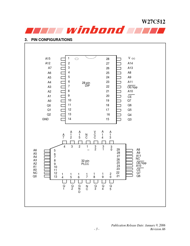
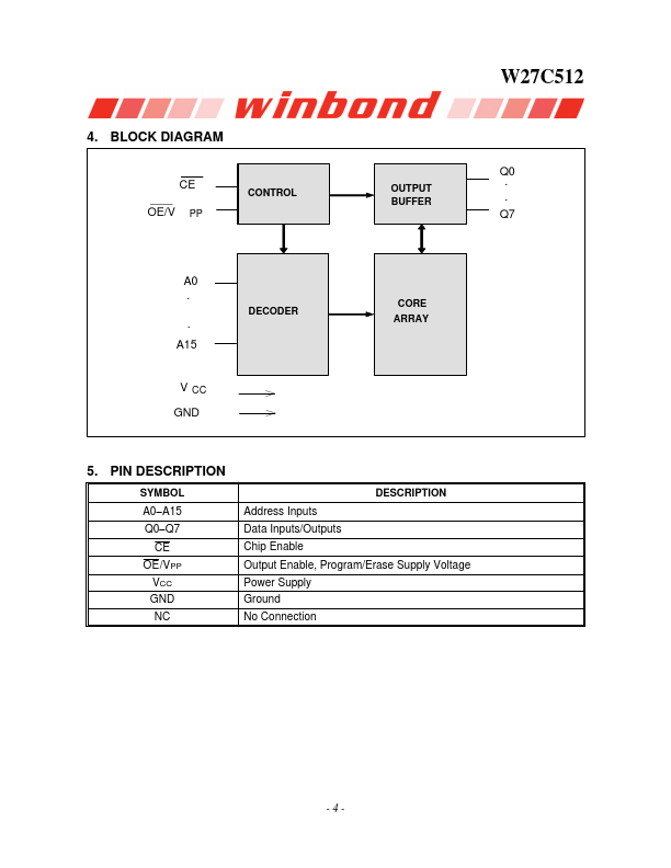
y High speed access time: 45/70/90/120 nS (max.) y Read operating current: 30 mA (max.) y Erase/Programming operating current: 30 mA (max.) y Standby current: 1 mA (max.) y Single 5V power supply y +14V erase/+12V programming voltage y Fully static operation y All inputs and outputs directly TTL/CMOS compatible y Three-state outputs y Available packages: 28-pin 600 mil DIP, 330 mil 32-pin PLCC -2- 3. PIN CONFIGURATIONS W27C512 A15 A12 A7 A6 A5 A4 A3 A2 A1 A0 Q0 Q1 Q2 GND 1 28 2 27 3 26 4 25 5 24 6 28-pin 23 7 DIP 22 8 21 9 20 10 19 11 18 12 17 13 16 14 15 V CC A14 A13 A8 A9 A11 OE/Vpp A10 CE Q7 Q6 Q5 Q4 Q3 A A1 72 A 1N 5C VAA C1 1 C4 3 432 1 3 3 3 A6 5 2 1 0 29 A8 A5 6 A4 7 A3 8 A2 9 A1 10 A0 11 32-pin PLCC 28 A9 27 A11 26 NC 25 OE/Vpp 24 A10 23 CE NC Q0 12 1 13 4 11 56 11 78 1 2 22 9 0 21 Q7 Q6 Q QG N Q Q Q 1 2NC 3 4 5 D Publication Release Date: January 9, 2006 -3- Revision A6 4. BLOCK DIAGRAM CE OE/V PP CONTROL W27C512 Q0 OUTPUT . BUFFER . Q7 A0 . . A15 V CC GND DECODER CORE ARRAY 5. Winbond Electronics Corporation