ABSOLUTE MAXIMUM RATINGS
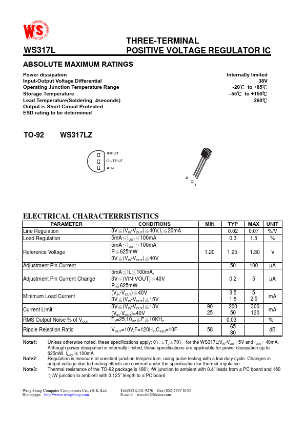
TO-92 WS317LZ INPUT OUTPUT ADJ A O I ELECTRICAL CHARACTERRISTISTICS PARAMETER Line Regulation Load Regulation Reference Voltage Adjustment Pin Current Adjustment Pin Current Change Minimum Load Current Current Limit RMS Output Noise % of VOUT Ripple Rejection Ratio Note1: Note2: Note3: CONDITIONS 3V≦(VIN-VOUT)≦40V,IL≦20mA 5mA≦IOUT≦100mA 5mA≦IOUT≦100mA P≦625mW 3V≦(VIN-VOUT)≦40V 5mA≦IL≦100mA, 3V≦(VIN-VOUT)≦40V P≦625mW (VIN-VOUT)≦40V 3V≦(VIN-VOUT)≦15V 3V≦(VIN-VOUT)≦13V (VIN-VOUT)=40V TJ=25,10HZ≦F≦10KHZ VOUT=10V,F=120HZ,CADJ=10F MIN TYP 0.02 0.3 1.25 50 0.2 3.5 1.5 200 50 0.03 65 80 MAX 0.07 1.5 1.30 100 5 5 2.5 300 120 UNIT %/V % V µA µA mA mA % dB 1.20 90 25 58 Unless otherwise noted, these specifications apply: 0℃≦TJ≦70℃ for the WS317L;VIN-VOUT=5V and IOUT= 40mA. Although power dissipation is internally limited, these specifications are applicable for power dissipation up to 625mW. IMAX is 100mA Regulation is measure at constant junction temperature, using pulse testing with a low duty cycle. Wing Shing Computer Components