YD324
YD324 is FOUR OPERATIONAL AMPLIFIER manufactured by Wuxi Youda electronics.
DESCRIPTION
AND FEATURES
These devices consist of four independent high-gain, phase
- pensated operational amplifiers. A suitable recorder and Audio System for tone control. Can also used for tele and instrument.
- Built-in phase-pensated circuit
- Operating supply voltage range : VCC =3.0~30.0V or VCC=±1.5~±15V
- Input voltage can low to 0V
- Output voltage range :0V~VCC-1.5V
- Supply current : ICC=0.6m A (RL=∞)
- DIP14 and SOP14
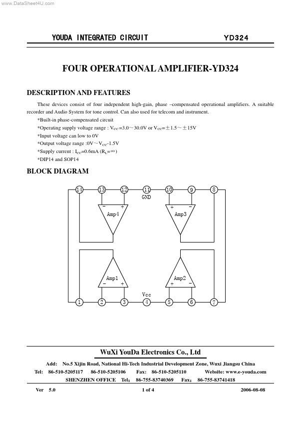
BLOCK DIAGRAM
14 13 Amp4 12 + 11 GND 10 + Amp3 9 8
Amp1 1 2 + 3 Vcc 4 5 +
Amp2
6 7
Wu Xi You Da Electronics Co., Ltd
Add: No.5 Xijin Road, National Hi-Tech Industrial Development Zone, Wuxi Jiangsu China Tel: 86-510-5205117 86-510-5205106 Fax: 86-510-5205110 Website: .e-youda. SHENZHEN OFFICE Tel: 86-755-83740369 Fax: 86-755-83741418 Ver 5.0 1 of 4 2006-08-08
..
YOUDA INTEGRATED CIRCUIT
PIN DESCRIPTION
PIN NO. 1 2 3 4 5 6 7 CONTENT Output of CH1 Inverting Input of CH1 Non-inverting Input of CH1 Supply Voltage Non-inverting Input of CH2 Inverting Input of CH2 Output of CH2 SYMBOL OUT1 1N-(1) 1N+(1) VCC 1N+(2) 1N-(2) OUT2 PIN NO. 8 9 10 11 12 13 14 CONTENT
SYMBOL OUT3 1N-(3) 1N+(3) GND 1N+(4) 1N-(4) OUT4
Output of CH3 Inverting Input of CH3 Non-inverting Input of CH3 Ground Non-inverting Input of CH4 Inverting Input of CH4 Output of CH4
ABSOLUTE MAXIMUM RATINGS
PARAMETER Supply Voltage Differential Input Voltage Input Voltage Total Dissipation(DIP14) Total Dissipation(SOP14) Operating Temperature Range Storage Temperature Range VALUE SYMBOL VCC VID VI PD1 PD2 Topr Tstg -30 -55 -0.3 MIN MAX 32 32 32 720 300 85 125 UNIT V V V m W m W ℃ ℃
ELECTRICAL CHARACTERISTICS (Tamb=25℃, VCC=9V, Unless otherwise specified)
PARAMETER Input Offset Voltage Input Offset Current Input Bias Current mon-mode Input Voltage Range mon-mode Rejection Ratio Open Loop Voltage Gain Output Voltage Range SYMBOL VIO IIO IIB VICM KCm R AVO VO VCC=15V, RL≥2kΩ 0 65 88 0 80 d B 100 VCC-1.5 V TEST CONDITION MIN TYP ±2 ±5 45 MAX ±7 ±50 250 VCC-1.5 UNIT mv n A V
Wu Xi You Da...