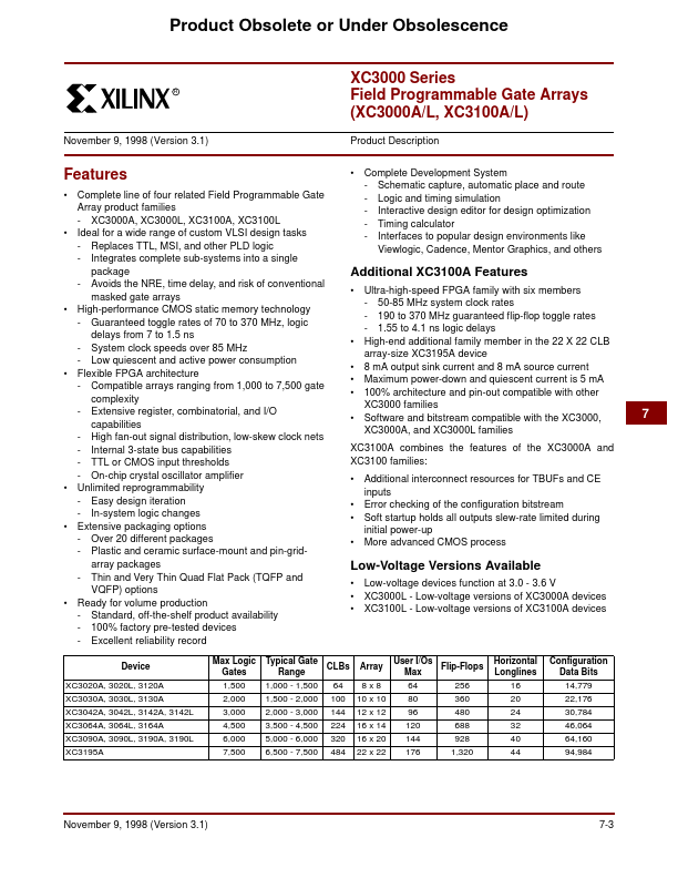
XC3090
Overview
- Complete line of four related Field Programmable Gate Array product families - XC3000A, XC3000L, XC3100A, XC3100L
- Ideal for a wide range of custom VLSI design tasks - Replaces TTL, MSI, and other PLD logic - Integrates complete sub-systems into a single package - Avoids the NRE, time delay, and risk of conventional masked gate arrays
- High-performance CMOS static memory technology - Guaranteed toggle rates of 70 to 370 MHz, logic delays from 7 to 1.5 ns - System clock speeds over 85 MHz - Low quiescent and active power consumption
- Flexible FPGA architecture - Compatible arrays ranging from 1,000 to 7,500 gate complexity - Extensive register, combinatorial, and I/O capabilities - High fan-out signal distribution, low-skew clock nets - Internal 3-state bus capabilities - TTL or CMOS input thresholds - On-chip crystal oscillator amplifier
- Unlimited reprogrammability - Easy design iteration - In-system logic changes
- Extensive packaging options - Over 20 different packages - Plastic and ceramic surface-mount and pin-gridarray packages - Thin and Very Thin Quad Flat Pack (TQFP and VQFP) options
- Ready for volume production - Standard, off-the-shelf product availability - 100% factory pre-tested devices - Excellent reliability record
- Complete Development System - Schematic capture, automatic place and route - Logic and timing simulation - Interactive design editor for design optimization - Timing calculator - Interfaces to popular design environments like Viewlogic, Cadence, Mentor Graphics, and others Additional XC3100A Features
- Ultra-high-speed FPGA family with six members - 50-85 MHz system clock rates - 190 to 370 MHz guaranteed flip-flop toggle rates - 1.55 to 4.1 ns logic delays
- High-end additional family member in the 22 X 22 CLB array-size XC3195A dev